Non-Volatile Memory Arrays Comprising Rail Stacks with a Shared Diode Component Portion for Diodes of Electrically Isolated Pillars

a non-volatile memory array and diode component technology, which is applied in the direction of bulk negative resistance effect devices, instruments, semiconductor devices, etc., can solve problems such as a wide range of difficulties

Active Publication Date: 2009-12-17
SANDISK TECH LLC
View PDF31 Cites 89 Cited by
  • Summary
  • Abstract
  • Description
  • Claims
  • Application Information

AI Technical Summary

Problems solved by technology

These processes can present a range of difficulties.

Method used


Image

  • Non-Volatile Memory Arrays Comprising Rail Stacks with a Shared Diode Component Portion for Diodes of Electrically Isolated Pillars
  • Non-Volatile Memory Arrays Comprising Rail Stacks with a Shared Diode Component Portion for Diodes of Electrically Isolated Pillars
  • Non-Volatile Memory Arrays Comprising Rail Stacks with a Shared Diode Component Portion for Diodes of Electrically Isolated Pillars

Examples


Embodiment Construction

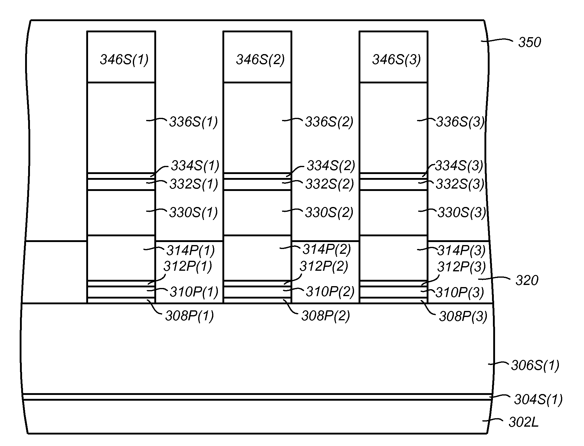
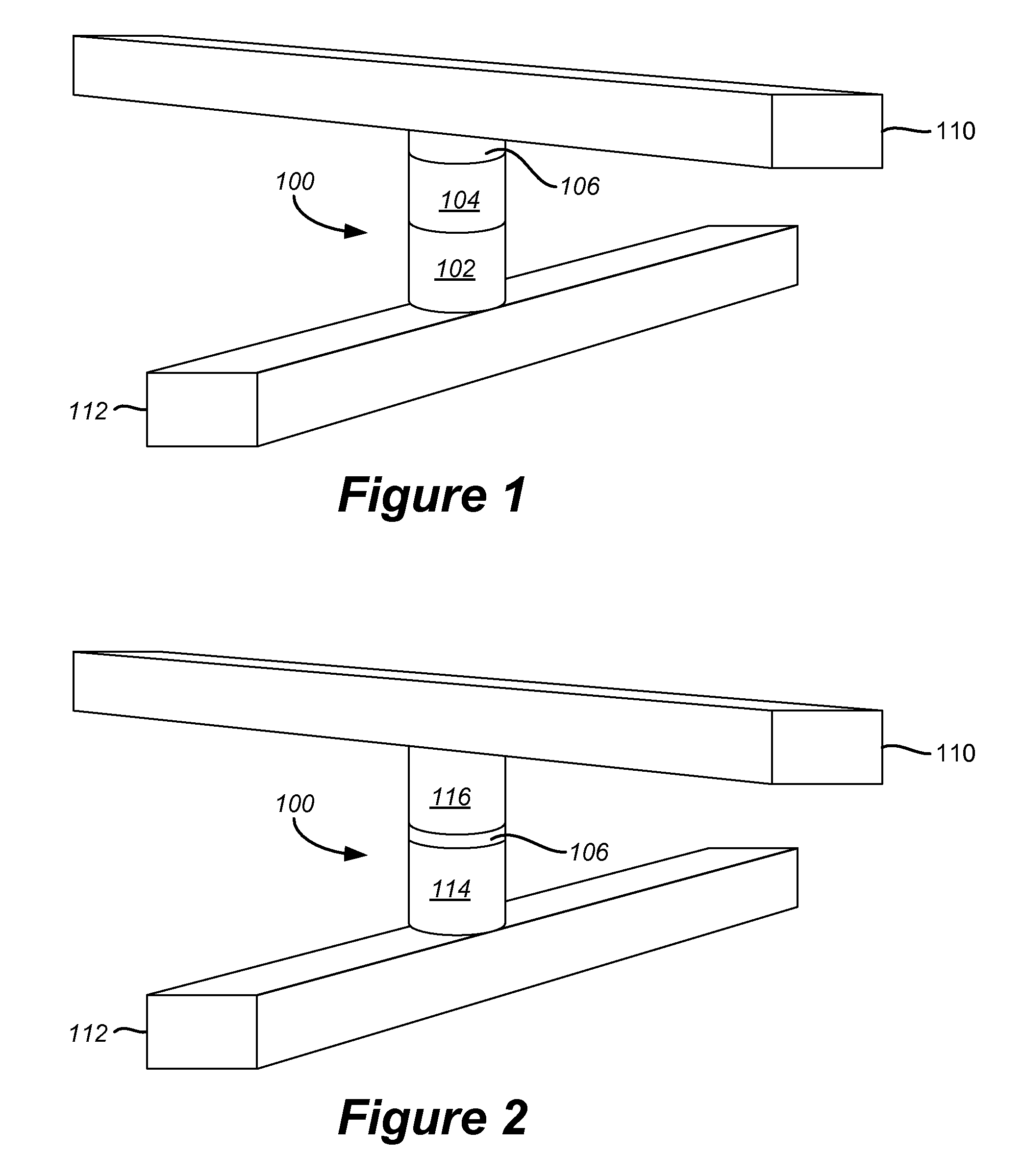
[0022]FIG. 1 depicts an exemplary structure of a two-terminal non-volatile memory cell including a pillar 100 of layers formed at an intersection between upper and lower conductors. A first terminal portion of the memory cell is connected to a first conductor 110 and a second terminal portion of the memory cell is connected to a second conductor 112. The memory cell is co-extensive with pillar 100, including a steering element 102 in series with a state change element 104 and an anti-fuse 106 to provide non-volatile date storage.

[0023]The steering element can take the form of any suitable device exhibiting a nonlinear conduction current characteristic such as a simple diode. The state change element will vary by embodiment and can include numerous types of materials to store data through representative physical states. State change element 104 can include resistance change materials, phase change resistive materials, etc. A semiconductor or other material having at least two levels ...


PUM


Abstract

An integrated circuit including vertically oriented diode structures between conductors and methods of fabricating the same are provided. Two-terminal devices such as passive element memory cells can include a diode steering element in series with an antifuse and/or other state change element. The devices are formed using pillar structures at the intersections of upper and lower sets of conductors. The height of the pillar structures are reduced by forming part of the diode for each pillar in a rail stack with one of the conductors. A diode in one embodiment can include a first diode component of a first conductivity type and a second diode component of a second conductivity type. A portion of one of the diode components is divided into first and second portions with one on the portions being formed in the rail stack where it is shared with other diodes formed using pillars at the rail stack.

Description

BACKGROUND OF THE INVENTION[0001]1. Field of the Invention[0002]Embodiments in accordance with the present disclosure are directed to integrated circuits containing non-volatile memory cell arrays and particularly those arrays incorporating passive element memory cells.[0003]2. Description of the Related Art[0004]Materials having a detectable level of change in state, such as a resistance or phase change, are used to form various types of non-volatile semiconductor based memory devices. For example, simple antifuses are used for binary data storage in one time field-programmable (OTP) memory arrays by assigning a lower resistance initial physical state of a memory cell to a first logical state such as logical ‘0,’ and assigning a higher resistance physical state of the cell to a second logical state such as logical ‘1.’ Some materials can have their resistance switched back in the direction of their initial resistance. These types of materials can be used to form re-writable memory ...

Claims


Application Information

Patent Timeline
Patent Type & Authority Applications(United States)
IPC IPC(8): H01L29/06H01L29/10G11C11/00H01L21/82
CPCH01L27/1021H10B63/20H10B63/80
Inventor HSIA, KANG-JAYPETTI, CHRISTOPHER J.LI, CALVIN K.
Owner SANDISK TECH LLC
Why Eureka
Try Eureka