Plasma display panel

a technology of display panel and plasma, which is applied in the direction of gas discharge vessel/container, gas-filled discharge tube, electrode, etc., can solve the problems of insufficient light blocking function, difficult to uniformly accumulate wall charges within the discharge cell, poor contact, etc., to reduce black luminance, improve contrast, and simplify manufacturing process

Inactive Publication Date: 2009-12-24
UTI LLP +1
View PDF8 Cites 0 Cited by
  • Summary
  • Abstract
  • Description
  • Claims
  • Application Information

AI Technical Summary

Benefits of technology

[0013] Embodiments of the present invention provide a plasma display panel capable of easily uniformly accumulating wall charge by preventing edge curl and improving contrast by reducing black luminance.
[0014] The embodiments of the present invention also provide a plasma display panel with improved contrast that can be manufactured in a simplified and less costly manner.
[0018] In the plasma display panel according to the embodiments of the present invention, the edge curl is prevented and the wall charges uniformly are accumulated by forming the bus electrode more narrowly than the width of the black layer. Further contrast is improved by reducing black luminance.
[0019] The plasma display panel according to the embodiments of the present invention simplifies the manufacturing process and reduces the manufacturing cost.

Problems solved by technology

A poor contact occurs where the bus electrode contacts the black layer.
It is difficult to uniformly accumulate wall charges within the discharge cell.
Further, the black layer insufficiently performs the light blocking function and insufficiently improves the color purity and the contrast.

Method used


Image

  • Plasma display panel
  • Plasma display panel
  • Plasma display panel

Examples


first embodiment

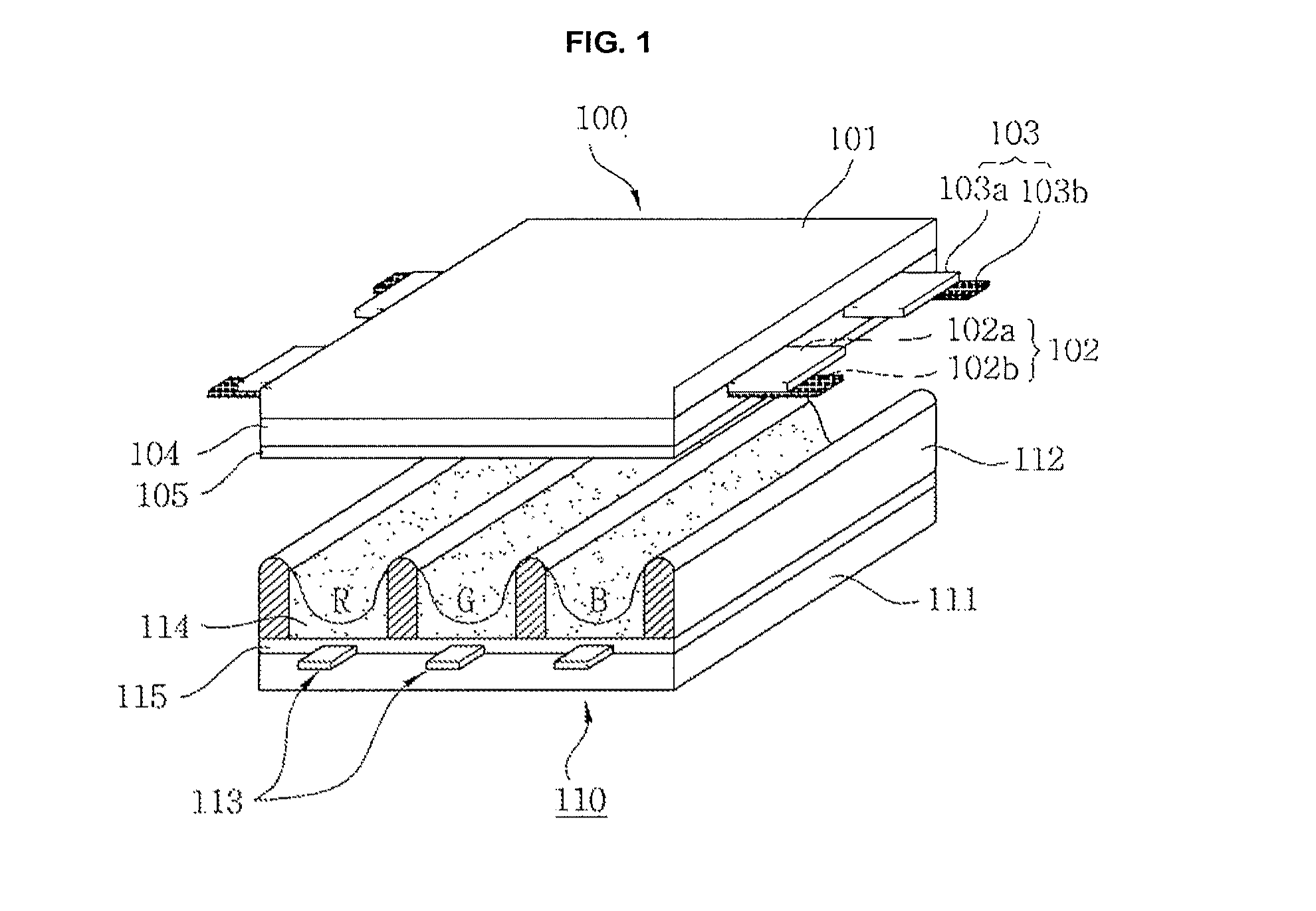
[0047]FIG. 1 shows a plasma display panel according to the present invention.

[0048] As shown in FIG. 1, the plasma display panel according to the first embodiment of the present invention comprises a front panel 100 and a rear panel 110 which are coupled in parallel to be opposed to each other at a given distance therebetween.

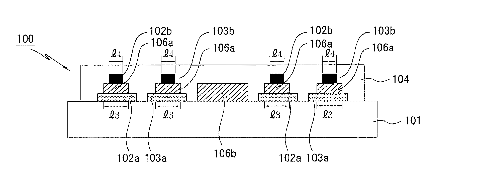
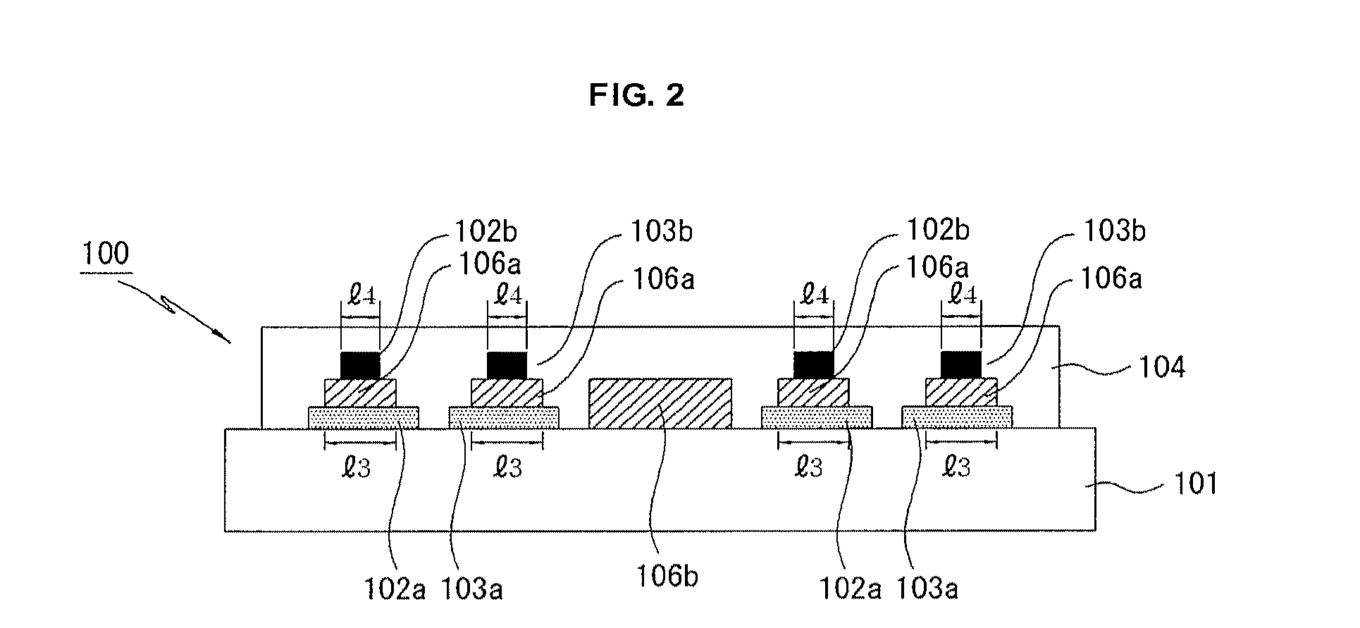
[0049] A plurality of scan electrodes 102 and a plurality of sustain electrodes 103 are formed in pairs on a front glass substrate 101 of the front panel 100 to form a plurality of maintenance electrode pairs.

[0050] The scan electrode 102 and the sustain electrode 103 each comprise transparent electrodes 102a and 103a made of transparent indium-tin-oxide (ITO) material and bus electrodes 102b and 103b made of a metal material. The scan electrode 102 and the sustain electrode 103 generate a mutual discharge therebetween in one discharge cell and maintain light-emissions of discharge cells.

[0051] The scan electrode 102 and the sustain electrode 103 are covered...

second embodiment

[0074]FIG. 4 is a schematic cross-sectional view of a front panel of a plasma display panel according to the present invention.

[0075] As shown in FIG. 4, a plurality of maintenance electrode pairs are arranged in parallel on a front glass substrate 401 of a front panel 400. The maintenance electrode pair comprise transparent electrodes 402a and 403a made of ITO material and bus electrodes 402b and 403b made of a metal material such as Ag on the transparent electrodes 402a and 403a.

[0076] Black layers 406a and 406b made of an electrically conductive material each are formed between the transparent electrodes 402a and 403a and the bus electrodes 402b and 403b.

[0077] The Black layer 406a and 406b are formed to be extended from a non-discharge region between discharge cells to a region between the transparent electrodes 402a and 403a and the bus electrodes 402b and 403b of a discharge cell adjacent to the non-discharge region. The Black layers 406a and 406b perform a light blocking fu...

third embodiment

[0094]FIG. 6 is a schematic cross-sectional view of a front panel of a plasma display panel according to the present invention.

[0095] As shown in FIG. 6, a plurality of maintenance electrode pairs comprising bus electrodes 602b and 603b made of a metal material such as Ag are arranged in parallel on a front glass substrate 601 of a front panel 600.

[0096] Since an expensive transparent electrode is not formed on the front panel 600 of the plasma display panel according to the third embodiment of the present invention unlike the front panel 100 of the plasma display panel according to the first embodiment of the present invention, the manufacturing cost of the plasma display panel decreases.

[0097] Black layers 606a and 606b made of an electrically conductive material are formed on the front glass substrate 601 of the front panel 600. The Black layers 606a and 606b perform a light blocking function for reducing reflectivity by absorbing external light generated from the outside of th...


PUM


Abstract

A plasma display panel is provided. The plasma display panel includes a front glass substrate, a transparent electrode formed on the front glass substrate, a black layer formed on an upper part of the transparent electrode, and a bus electrode formed on an upper part of the black layer. The width of the bus electrode is less than the width of the black layer.

Description

[0001] This Nonprovisional application claims priority under 35 U.S.C. § 119(a) on Patent Application No. 2005-0039293 filed in Korea on May 11, 2005 the entire contents of which are hereby incorporated by reference. BACKGROUND OF THE INVENTION [0002] 1. Field of the Invention [0003] This document relates to a display apparatus, and more particularly, to a plasma display apparatus. [0004] 2. Description of the Background Art [0005] Out of display apparatuses, a plasma display apparatus generally comprises a plasma display panel and a driver for driving the plasma display panel. [0006] The plasma display panel comprises a front panel and a rear panel which are made of soda-lime glass. Barrier ribs formed between the front panel and the rear panel form discharge cells. Each of the discharge cells is filled with an inert gas such as a He—Xe gas mixture, a He—Ne gas mixture. When the inert gas is discharged by a high frequency voltage, vacuum ultraviolet rays are generated. Vacuum ultra...

Claims


Application Information

Patent Timeline
Patent Type & Authority Applications(United States)
IPC IPC(8): H01J17/49H01J11/12H01J11/22H01J11/24H01J11/26H01J11/34H01J11/36H01J11/38H01J11/40H01J11/42H01J11/44H01J11/50
CPCH01J11/12H01J2211/444H01J2211/245H01J11/24H01J11/44
Inventor CHUNG, MIN
Owner UTI LLP
Why Eureka
Try Eureka