Display panel substrate, display panel, display appratus, and method for manufacturing display panel substrate

a technology of display panel and substrate, applied in the field of display panel substrate, display panel, display panel, display appratus, etc., can solve the problems of increasing the size of the display apparatus and the size of the display panel, and achieve the effect of increasing the aperture ratio

Inactive Publication Date: 2010-01-21
SHARP KK
View PDF12 Cites 84 Cited by
  • Summary
  • Abstract
  • Description
  • Claims
  • Application Information

AI Technical Summary

Benefits of technology

[0040]The arrangement makes it possible to realize the display panel substrate as a drive substrate.
[0041]Overlapping the first conductive wires and the second conductive wires on the source wires and the gate wires, respectively, is carried out by use of a high-accuracy stepper o...

Problems solved by technology

This causes an increase in size of the picture frame of the substra...

Method used


Image

  • Display panel substrate, display panel, display appratus, and method for manufacturing display panel substrate
  • Display panel substrate, display panel, display appratus, and method for manufacturing display panel substrate
  • Display panel substrate, display panel, display appratus, and method for manufacturing display panel substrate

Examples


example 1

of Arrangement / Manufacturing Steps

Steps of Manufacturing Counter Substrate

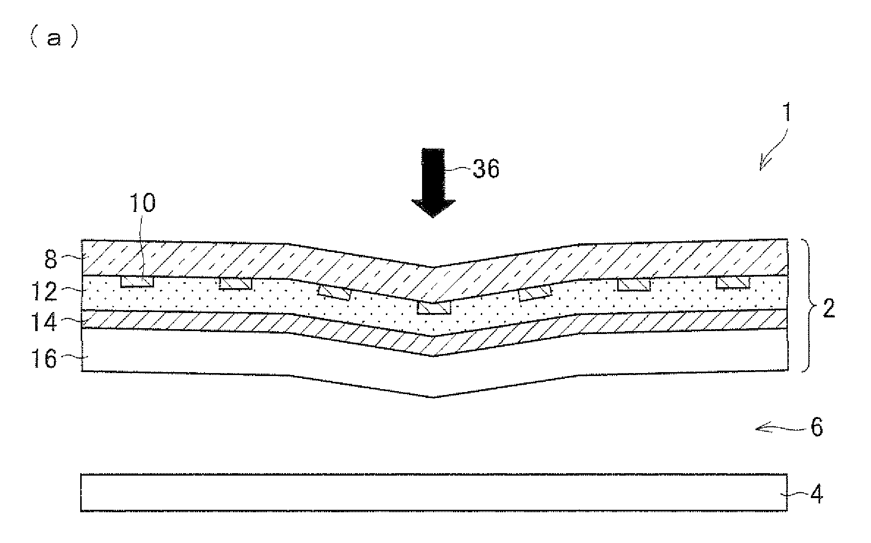
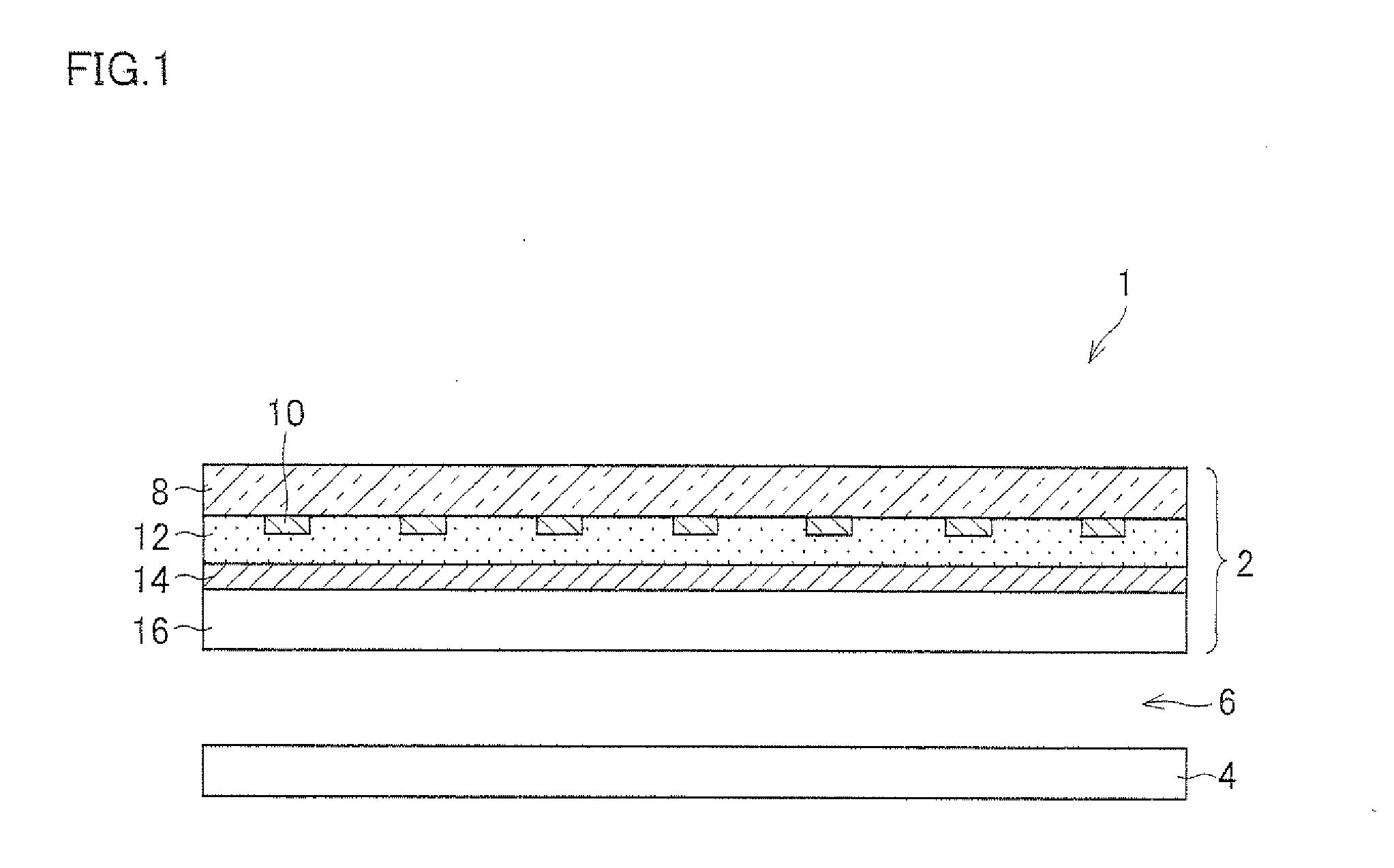
[0166](a) through (d) of FIG. 8 and (a) through (d) of FIG. 9 illustrate steps of manufacturing the counter substrate 2 of FIG. 7. (a) through (d) of FIG. 8 are diagrams illustrating the steps of manufacturing the counter substrate 2 illustrated in FIG. 7. (a) through (d) of FIG. 9 are cross-sectional views illustrating the steps of manufacturing the counter substrate 2 illustrated in FIG. 7. A cross section taken along the line A-A′ of (d) of FIG. 8 corresponds to (d) of FIG. 9. (a) through (c) of FIG. 8 correspond to (a) through (c) of FIG. 9, respectively, as is the case with the relation between (d) of FIG. 8 and (d) of FIG. 9.

[0167]In the manufacture of the counter substrate 2 of FIG. 7, first, the metal wires 10 are formed on the glass substrate 8 (see (a) of FIG. 8 and (a) of FIG. 9). Specifically, a metal film made of metal such as titanium is formed on the glass substrate 8 by DC magnetron sputtering ...

example 2

of Arrangement / Manufacturing Steps

Example of Case where Opening is Provided at Least in Display Area Surrounded by Wires

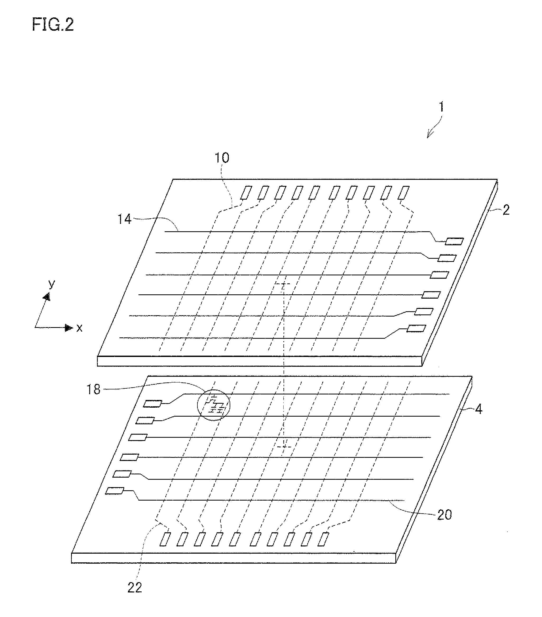
[0179]From a viewpoint of transmittance, it is advantageous to provide an opening at least in a display area surrounded by two metal wires 10 and two metal wires 14. Furthermore, it is preferable to form a piezoelectric film 12 at an intersection of each metal wire 10 and each metal wire 14. FIG. 10 illustrates a counter substrate 2 thus arranged. (a) of FIG. 10 is a diagram illustrating a structure of the counter substrate 2. (b) of FIG. 10 is a cross-sectional view taken along the line A-A′ of (a) of FIG. 10.

[0180]In the case of the counter substrate 2 of FIG. 10, no piezoelectric films 12 are formed in areas each surrounded by two metal wires 10 and two metal wires 14. This makes it possible to increase light transmittance, in comparison with a case where piezoelectric films 12 are formed in the areas. Therefore, it is possible to reduce the amount of light with...

example 3

of Arrangement / Manufacturing Steps

Second Example of Case where Opening is Provided at Least in Display Area Surrounded by Two Metal Wires 10 and Two Metal Wires 14

[0193]Example 2 described above has more manufacturing steps than Example 1. Therefore, it is desirable to simplify the steps. For example, patterning piezoelectric films 12 by use of metal wires 14 as a mask makes it possible to manufacture the counter substrate 2 by using the same number of masks as in Example 1. This makes it possible to improve yield and reduce manufacturing cost. FIG. 13 illustrates a counter substrate 2 thus arranged. (a) of FIG. 13 is a diagram illustrating a structure of a counter substrate 2 made through patterning of piezoelectric films 12 by use of metal wires 14 as a mask. (b) of FIG. 13 is a cross-sectional view taken along the line A-A′ of (a) of FIG. 13.

[0194]The counter substrate 2 of FIG. 13 makes it possible to simplify the manufacturing steps while improving light transmittance. This mak...


PUM


Abstract

A display panel substrate according to the present invention includes at least an insulating substrate, first conductive wires formed on the insulating substrate, a piezoelectric material film formed on the first conductive wires, second conductive wires intersecting with the first conductive wires, and a protecting film for protecting the first conductive wires, the second conductive wires, and the piezoelectric material film. The insulating film is formed at least in an area in an effective display area on the insulating substrate. The piezoelectric film is formed at least at an intersection of a first conductive wire and a second conductive wire. This makes it possible to provide a display panel substrate that allows integration of a touch panel function into a display panel without causing an increase in size of the display panel.

Description

TECHNICAL FIELD[0001]The present invention relates to a display panel substrate that constitutes a display panel, a display panel including the display panel substrate, a display apparatus including the display panel, and a method for manufacturing the display panel substrate.BACKGROUND ART[0002]Conventionally, a so-called touch panel has been commonly provided in a display apparatus so that a user can easily operate the display apparatus while viewing a display screen. A touch panel is generally joined with a display screen of a display apparatus. A user performs various operations by pushing (selecting), via a touch panel, objects (such as buttons) displayed on a display screen.[0003]Patent Literature 1 discloses a typical example of a touch panel to be attached to a display apparatus. Patent Literature 1 discloses a pressing-force detecting section (touch panel) arranged such that (i) a plurality of electrodes formed on one side of a piezoelectric body so as to extend in a direct...

Claims


Application Information

Patent Timeline
IPC IPC(8): G06F3/041
CPCG02F1/13338G06F3/047G06F3/0414G06F3/04146
Inventor MURAI, ATSUHITOCHIKAMA, YOSHIMASATAKAHASHI, KAZUKI
Owner SHARP KK
Why Eureka
Try Eureka