Semiconductor device, semiconductor module, method for manufacturing semiconductor device, and lead frame

Active Publication Date: 2010-02-04
SEMICON COMPONENTS IND LLC
View PDF8 Cites 14 Cited by
  • Summary
  • Abstract
  • Description
  • Claims
  • Application Information

AI Technical Summary

Benefits of technology

[0025]According to a semiconductor device and semiconductor module according to one aspect of the present invention, a main surface of a sealing resin has a part thereof pressed by pressing member depressed to form a depressed part. Moreover, this depressed part is formed in an area where the sealing resin superimposes a semiconductor element sealed with the sealing resin. This prevents pressing member such as a screw from pressing the main surface of the sealing resin that superimposes an area where the semiconductor element is disposed. As a result, a pressing force caused by the pr

Problems solved by technology

However, the above-mentioned semiconductor device 100 has a problem that the semiconductor element 104 could be destroyed by a pressing force of the screw that brings the semiconductor device 100 into contact with the heat sink.
In addition, when a thickness of the sealing resin 108 that covers the semiconductor element 104 is made thinner in order to obtain a low profile semiconductor device, the above-mentioned problem is more likely to occur.
Furthermore, the above-mentioned method for manufacturing the semiconductor device has a problem that the lower surface of the island 102 is not sufficiently covered with the sealing resin 108

Method used


Image

  • Semiconductor device, semiconductor module, method for manufacturing semiconductor device, and lead frame
  • Semiconductor device, semiconductor module, method for manufacturing semiconductor device, and lead frame
  • Semiconductor device, semiconductor module, method for manufacturing semiconductor device, and lead frame

Examples


first embodiment

[0044]In the present embodiment, description will be given on a semiconductor device and a method for manufacturing the semiconductor device in which a depressed part is provided in a sealing resin in order to prevent breakage of the semiconductor element due to an external force.

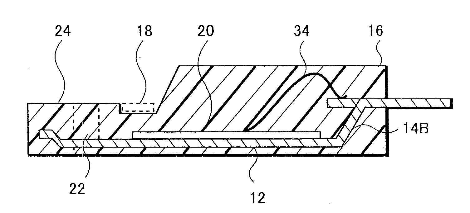
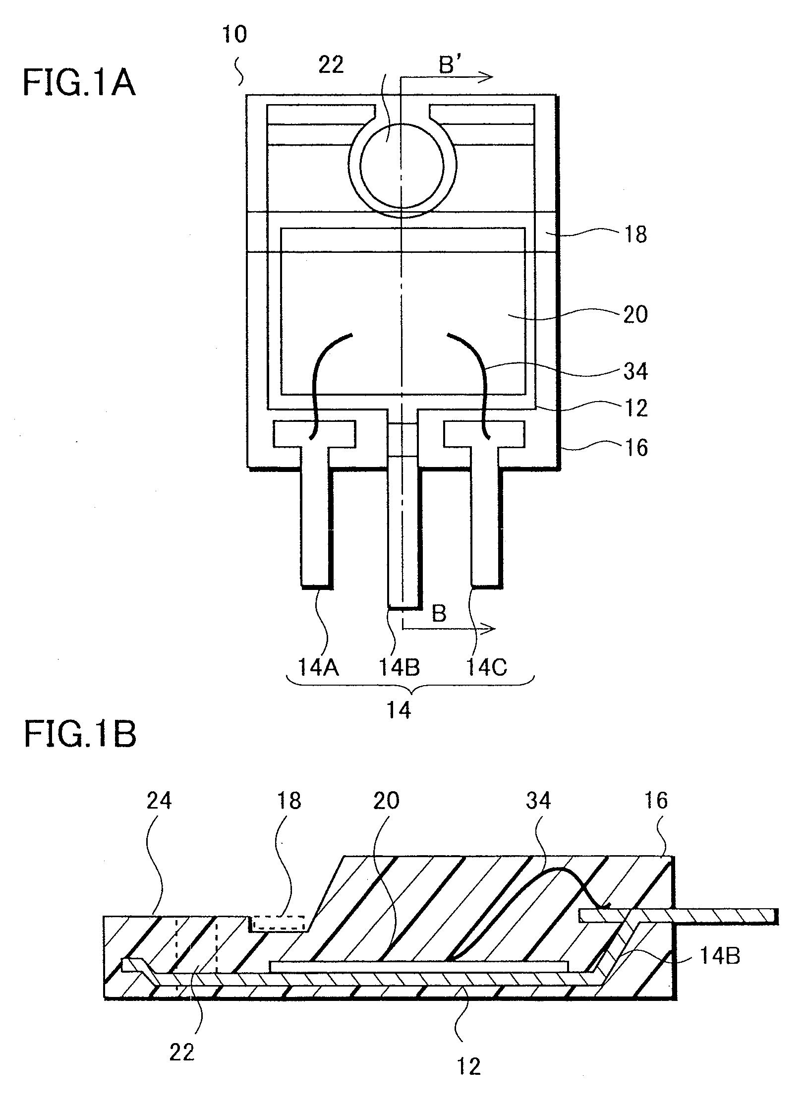
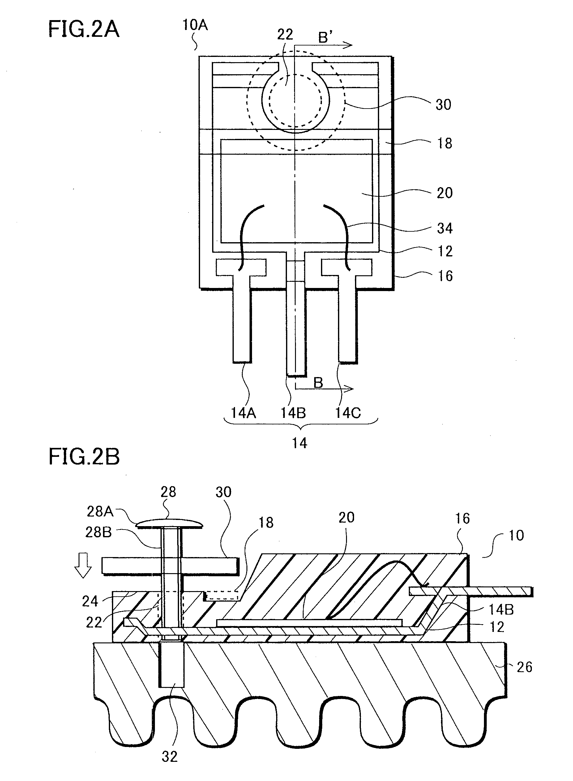
[0045]With reference to FIGS. 1A and 1B, a configuration of a semiconductor device 10 according to the present embodiment will be described. FIG. 1A is a plan view showing the semiconductor device 10, and FIG. 1B is a sectional view taken along the line B-B′ in FIG. 1A.

[0046]As shown in FIGS. 1A and 1B, the semiconductor device 10 has a configuration mainly including an island 12, a semiconductor element 20 mounted on a front surface of the island 12, a lead 14 that functions as an external connection terminal, and a sealing resin 16 that covers these components in an integrated manner and mechanically supports them.

[0047]The island 12 is obtained by forming a conductive foil made of a metal such as copper ...

second embodiment

[0070]In the present embodiment, description will be given on a method for manufacturing a semiconductor device and a lead frame used therein, in which an island provided with an inclined side surface is sealed with a resin.

[0071]With reference to FIGS. 8A to 8B and FIGS. 9A to 9C, a configuration of a lead frame 50 according to the present embodiment will be described.

[0072]FIG. 8A is a plan view showing the lead frame 50 as a whole, and FIG. 8B is a partially enlarged plan view of the lead frame 50.

[0073]With reference to FIG. 8A, an outline of the lead frame 50 is rectangular, and multiple units 56 are formed within a frame-like outer frame 52 and arranged in a matrix form.

[0074]FIG. 8B is a plan view in which FIG. 8A is partially enlarged. Here, tie bars 58 extend to continue to an upper outer frame 52 and a lower outer frame 52. The units 56A to 56D are arranged in a line on a left side in FIG. 8B and are connected to each other by the tie bars 58, and the units 56E to 56H are ...


PUM


Abstract

To provide a semiconductor device and a semiconductor module in which breakage of a semiconductor element due to a pressing force given from the outside is prevented. A semiconductor device according to the present invention has a configuration mainly including an island, a semiconductor element mounted on a front surface of the island, a lead that functions as an external connection terminal, and a sealing resin that covers these components in an integrated manner and mechanically supports them. Further, a through-hole is provided so as to penetrate the sealing resin. A front surface of the sealing resin around the through-hole forms a flat part. The front surface of the sealing resin that overlaps the semiconductor element is depressed inward with respect to the flat part to form a depressed part.

Description

[0001]This application claims priority from Japanese Patent Application Number JP 2008-195784 filed on Jul. 30, 2008, and Japanese Patent Application Number JP 2008-195785 filed on Jul. 30, 2008, the contents of which are incorporated herein by reference in their entirety.BACKGROUND OF THE INVENTION[0002]1. Field of the Invention[0003]The present invention relates to a semiconductor device and a semiconductor module, and particularly, relates to a lead frame type semiconductor device and semiconductor module in which a comparatively large-sized semiconductor element is sealed with a resin. The present invention further relates to a method for manufacturing a semiconductor device, and to a lead frame, and particularly relates to a method for manufacturing a semiconductor device and a lead frame in which a lower surface of an island on which a large-sized discrete type semiconductor element is mounted is sealed with a resin.[0004]2. Description of the Related Art[0005]Semiconductor de...

Claims


Application Information

Patent Timeline
IPC IPC(8): H01L23/495H01L23/28H01L23/34H01L21/60
CPCB29C45/0046B29C45/14065H01L2924/1305H01L2924/1306H01L2924/014H01L2924/01033H01L2924/01006H01L2924/01005H01L2924/1815H01L2924/13091H01L2924/13055H01L2924/01322H01L2924/01082H01L2924/01078H01L2924/01029H01L2924/01013H01L2224/97B29C45/14655B29C45/2628B29C45/2708H01L21/561H01L21/565H01L23/4006H01L23/49503H01L23/49562H01L24/48H01L24/97H01L2224/48091H01L2224/48247H01L2224/4847H01L2224/48472H01L2224/85H01L2924/00014H01L2924/00H01L2224/451H01L2924/181
Inventor SAKAI, HARUHIKO
Owner SEMICON COMPONENTS IND LLC
Why Eureka
Try Eureka