

Information storage system which includes a bonded semiconductor structure
a technology of information storage and semiconductors, applied in the direction of semiconductors, electrical devices, transistors, etc., can solve the problems of laterally oriented devices consuming significant chip area, complex and expensive to fabricate a computer chip with memory embedded in this way, and generally not compatible with the mask used
- Summary
- Abstract
- Description
- Claims
- Application Information
AI Technical Summary
Problems solved by technology
Method used
Image

Examples
Embodiment Construction
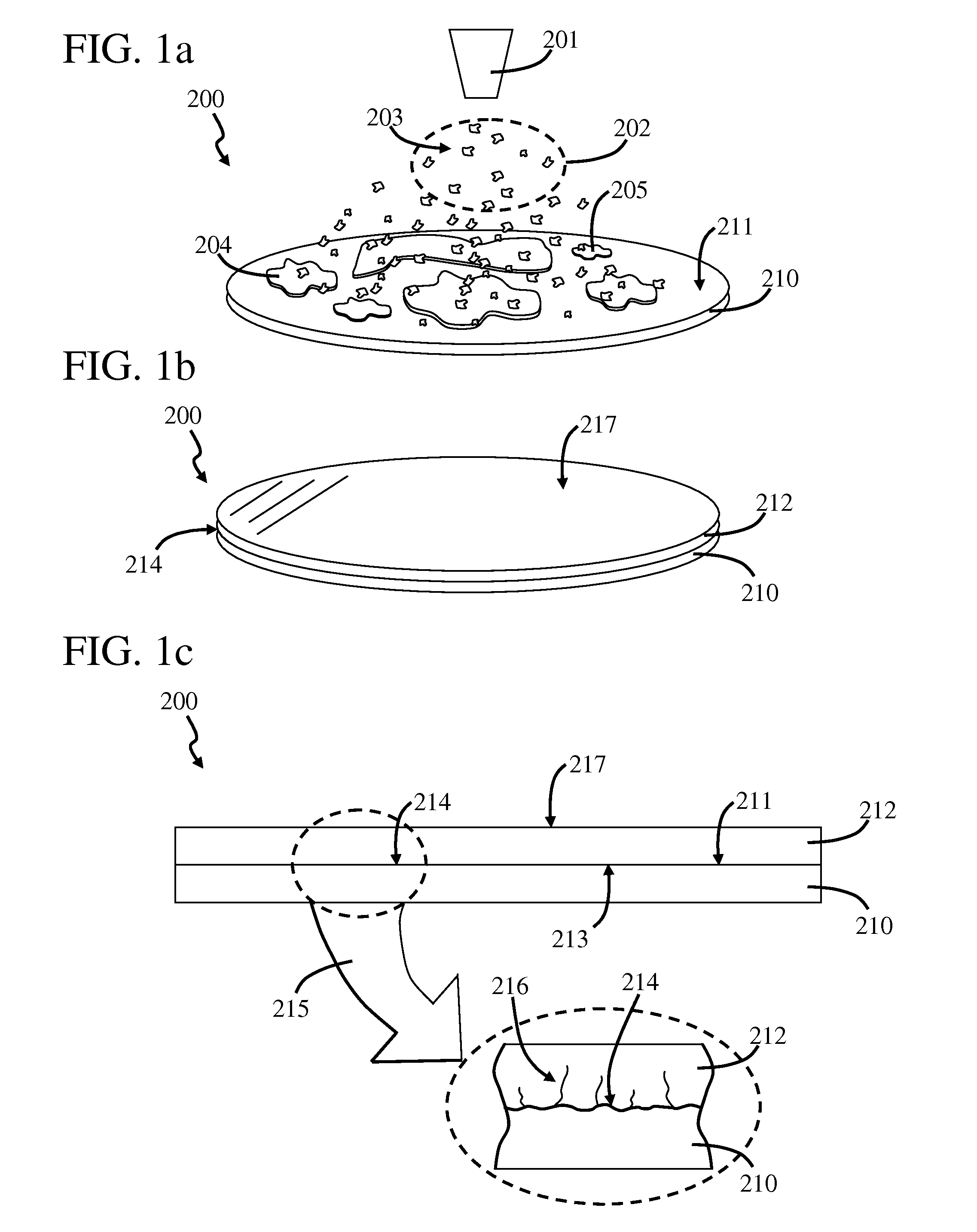
[0057]FIG. 1a is a perspective view of a partially fabricated grown semiconductor structure 200. Grown semiconductor structure 200 includes a substrate 210. Substrate 210 can be of many different types, such as a semiconductor substrate. A gaseous semiconductor material 203 is provided from a growth material source 201 in a region 202 proximate to a substrate surface 211 of substrate 210. It should be noted that, in general, more than one material sources are used to provide growth material and process gases. However, one material source is shown in FIG. 1a for simplicity and ease of discussion.
[0058]Portions of gaseous semiconductor material 203 engage surface 211 to form agglomerated semiconductor material 204 and 205. Portions of gaseous semiconductor material 203 engage surface 211 to form a grown semiconductor layer 212 on surface 211 of substrate 210, as shown in FIG. 1b, and a growth interface 214, as shown in FIG. 1c. FIG. 1b is a perspective view of substrate 210 and grown ...
PUM
 Abstract
Description
Claims
Application Information