Light emitting device and method of manufacturing the same

a technology of light emitting devices and manufacturing methods, which is applied in the manufacture of semiconductor/solid-state devices, semiconductor devices, electrical devices, etc., can solve the problems of deteriorating luminance of light emitting devices and the non-normal operation of emitting devices, and achieve the effect of damage to the epitaxial layer

Active Publication Date: 2010-03-11
SUZHOU LEKIN SEMICON CO LTD
View PDF2 Cites 13 Cited by
  • Summary
  • Abstract
  • Description
  • Claims
  • Application Information

AI Technical Summary

Benefits of technology

[0010]According to the embodiments, the damage of the epitaxial layer, which may be caused during a process for dividing the epitaxial layer into a plurality of light emitting devices, can be reduced.

Problems solved by technology

However, in the course of dividing the substrate and the epitaxial layer through the scribing process, the epitaxial layer may be damaged and thus the light emitting device does not normally operate or the luminance of the light emitting device is deteriorated.

Method used


Image

  • Light emitting device and method of manufacturing the same
  • Light emitting device and method of manufacturing the same
  • Light emitting device and method of manufacturing the same

Examples


Embodiment Construction

[0013]Reference will now be made in detail to the embodiments of the present disclosure, examples of which are illustrated in the accompanying drawings.

[0014]In the following description, it will be understood that when a layer (or film) is referred to as being “on” another layer or substrate, it can be directly on the other layer or substrate, or intervening layers may also be present. Further, it will be understood that when a layer is referred to as being “under” another layer, it can be directly under the other layer, and one or more intervening layers may also be present. In addition, it will also be understood that when a layer is referred to as being “between” two layers, it can be the only layer between the two layers, or one or more intervening layers may also be present.

[0015]In the figures, the dimensions of layers and regions are exaggerated for clarity of illustration. In addition, the dimension of each part does not reflect an actual size.

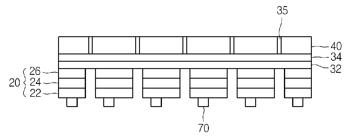
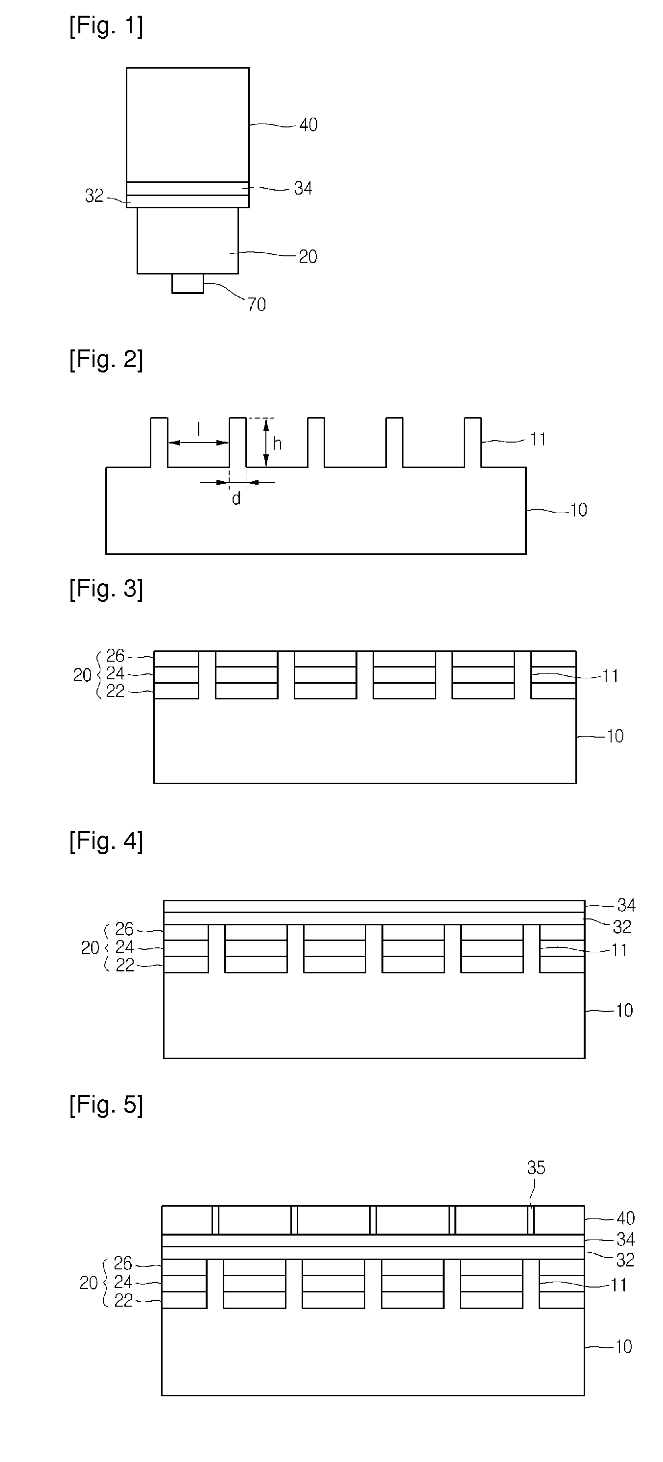
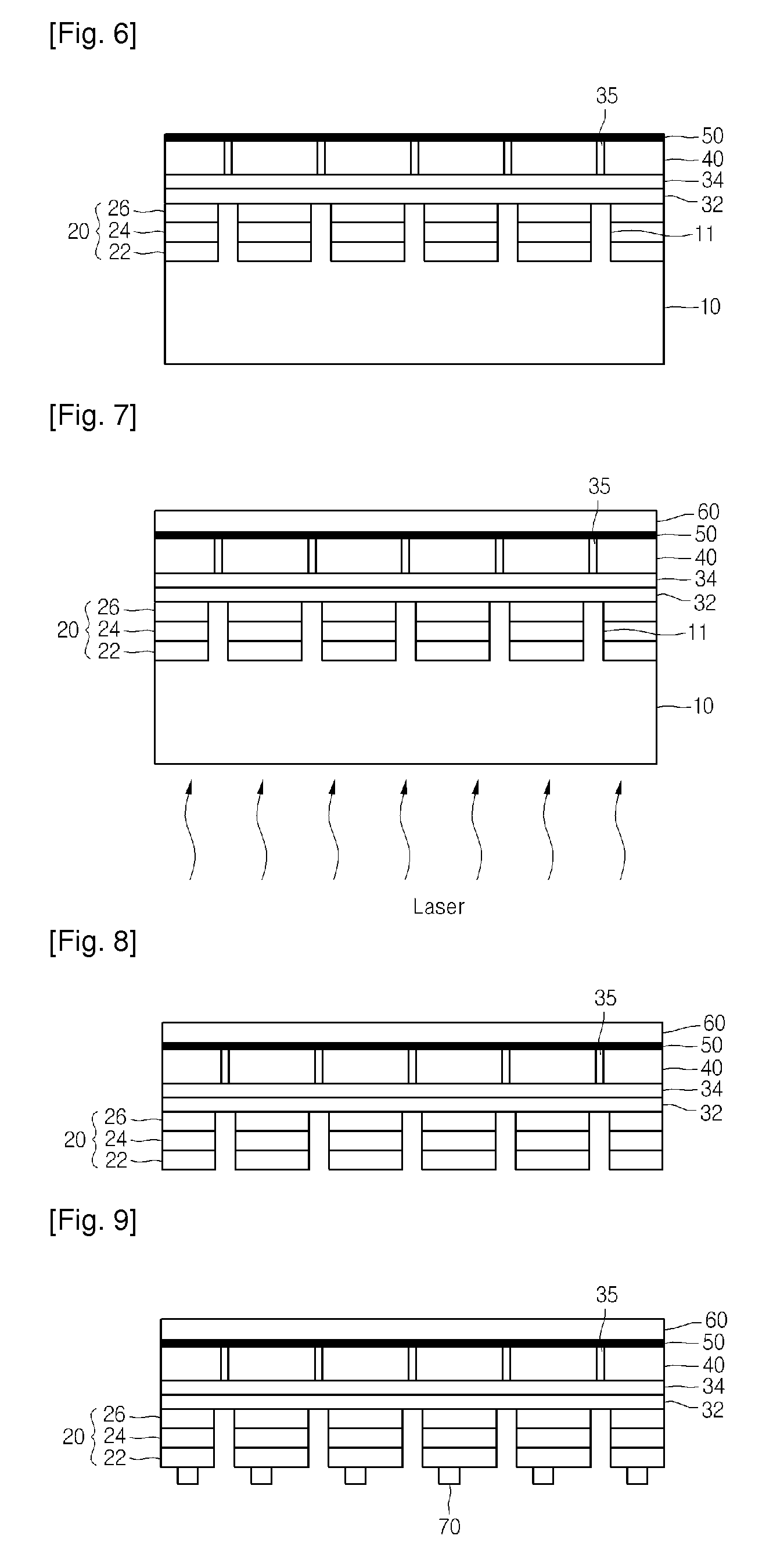
[0016]FIG. 1 is a schematic di...


PUM


Abstract

A method of manufacturing a light emitting device is provided. An epitaxial layer is first formed at a plurality of separated regions on a substrate and a second electrode layer is formed on the epitaxial layer. Subsequently, the substrate is removed from the epitaxial layer and a first electrode layer is formed under the epitaxial layer, after which the second electrode layer is divided into chip units.

Description

TECHNICAL FIELD[0001]The present disclosure relates to a light emitting device and a method of manufacturing the same.BACKGROUND ART[0002]A light emitting diode (LED) that can emit infrared rays or visible rays using a compound semiconductor is the representative of light emitting devices.[0003]The light emitting device includes a substrate, an epitaxial layer including a first conductive semiconductor layer, an active layer, and a second conductive semi-conductor layer on the substrate. The substrate and the epitaxial layer are divided into a plurality of chip units through a scribing process, thereby completing the light emitting device.[0004]However, in the course of dividing the substrate and the epitaxial layer through the scribing process, the epitaxial layer may be damaged and thus the light emitting device does not normally operate or the luminance of the light emitting device is deteriorated.DISCLOSURE OF INVENTIONTechnical Problem[0005]Embodiments provide a light emitting ...

Claims


Application Information

Patent Timeline
Patent Type & Authority Applications(United States)
IPC IPC(8): H01L33/00
CPCH01L33/007H01L33/0095H01L33/0079H01L33/0093
Inventor JEONG, HWAN HEE
Owner SUZHOU LEKIN SEMICON CO LTD
Why Eureka
Try Eureka