
Phase Change Memory Cell with MOSFET Driven Bipolar Access Device

a technology of bipolar access device and phase change memory cell, which is applied in semiconductor devices, digital storage, instruments, etc., can solve the problem that bipolar memory arrays require relatively large amounts of power

Inactive Publication Date: 2010-03-11
POLARIS INNOVATIONS
View PDF2 Cites 52 Cited by
  • Summary
  • Abstract
  • Description
  • Claims
  • Application Information

AI Technical Summary

Benefits of technology

[0010]These and other problems are generally solved or circumvented, and technical advantages are generally achieved, by preferred embodiments of the present invention in which an integrated circuit includes a first conta

Problems solved by technology

Additionally, such bipolar memory arrays require relatively large amounts of power.

Method used


Image

  • Phase Change Memory Cell with MOSFET Driven Bipolar Access Device
  • Phase Change Memory Cell with MOSFET Driven Bipolar Access Device
  • Phase Change Memory Cell with MOSFET Driven Bipolar Access Device

Examples


Embodiment Construction

[0025]In the following detailed description, reference is made to the accompanying drawings, which form a part hereof, and in which is shown by way of illustration specific embodiments in which the invention may be practiced. In this regard, directional terminology, such as “top,”“bottom,”“front,”“back,”“leading,”“trailing,” etc., is used with reference to the orientation of the Figure(s) being described. Because components of embodiments can be positioned in a number of different orientations, the directional terminology is used for purposes of illustration and is in no way limiting. It is to be understood that other embodiments may be utilized and structural or logical changes may be made without departing from the scope of the present invention. The following detailed description, therefore, is not to be taken in a limiting sense, and the scope of the present invention is defined by the appended claims. It is to be understood that the features of the various exemplary embodiments...


PUM


Abstract

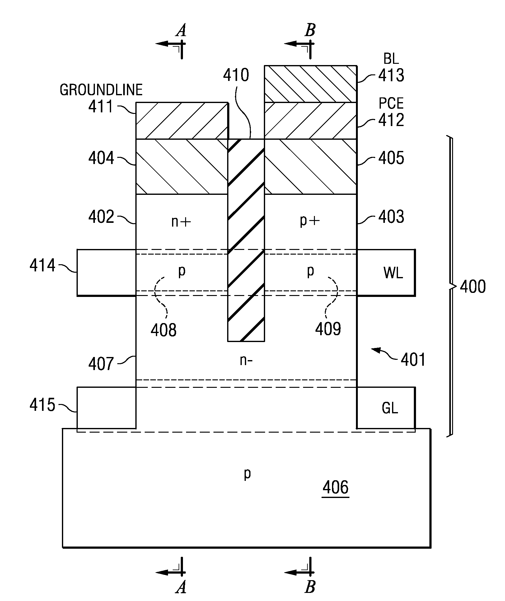
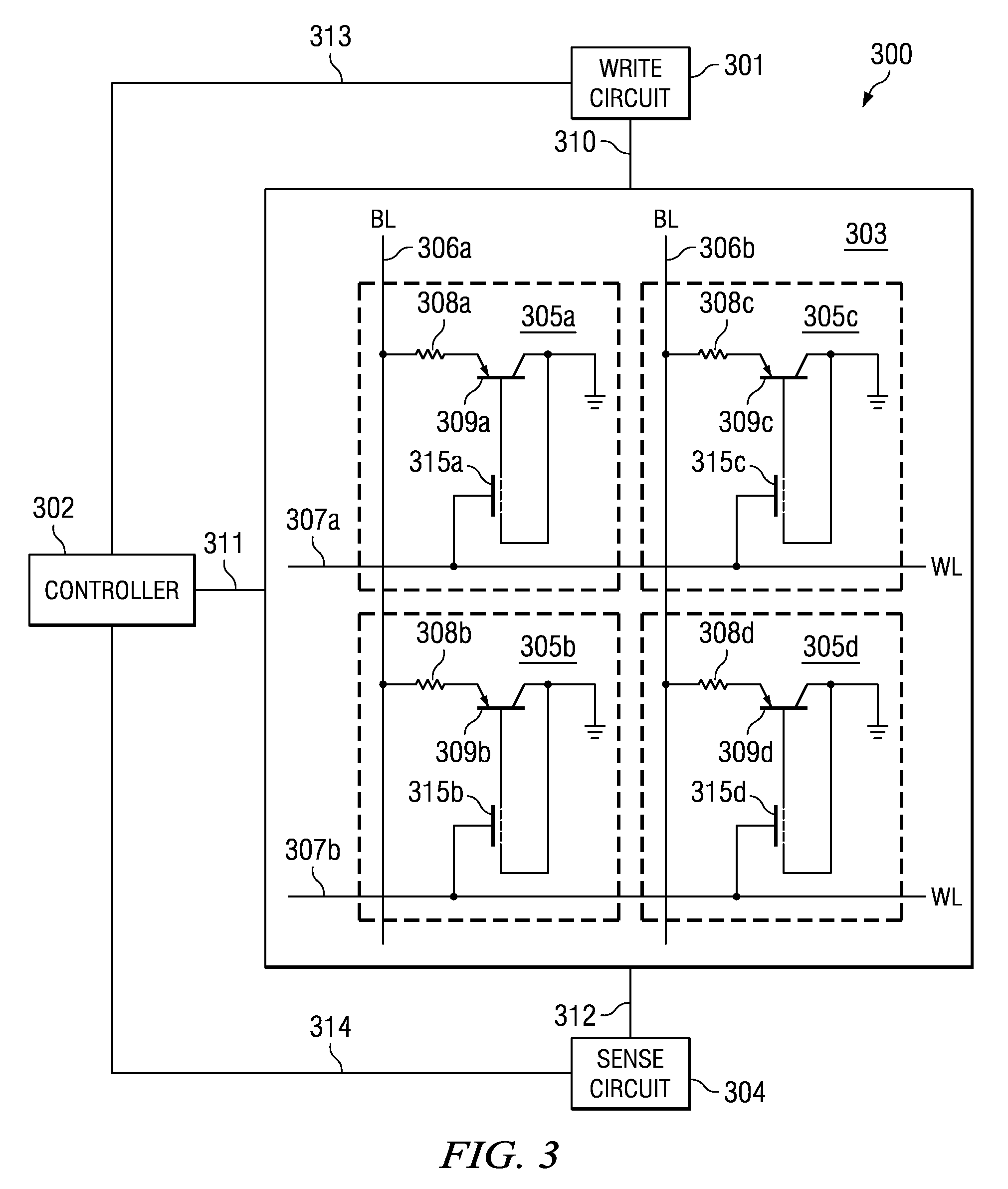
Embodiments are directed to memory devices comprising a bipolar junction transistor having an emitter, a base and a collector; a first side of a resistance changing memory element coupled to the emitter of the bipolar junction transistor; and a MOSFET coupled to the base of the bipolar junction transistor.

Description

CROSS-REFERENCE TO RELATED APPLICATIONS[0001]This application relates to the following co-pending and commonly assigned patent applications: U.S. patent application Ser. No. 12 / 033,519, filed Feb. 19, 2008, entitled “Integrated Circuit Including U-Shaped Access Device;” and U.S. patent application Ser. No. 12 / 033,533, filed Feb. 19, 2008, entitled “Integrated Circuit Including U-Shaped Access Device,” which applications are hereby incorporated herein by reference.TECHNICAL FIELD[0002]The present invention relates generally to phase change memory devices comprising MOSFET driven bipolar transistors.BACKGROUND[0003]One type of memory is resistive memory. Resistive memory utilizes the resistance value of a memory element to store one or more bits of data. For example, a memory element programmed to have a high resistance value may represent a logic “1” data bit value and a memory element programmed to have a low resistance value may represent a logic “0” data bit value. Typically, the ...

Claims


Application Information

Patent Timeline
IPC IPC(8): G11C11/00H01L21/00H01L47/00
CPCG11C13/0004G11C2213/72G11C2213/79H01L45/148H01L45/06H01L45/1233H01L45/144H01L27/2445H10B63/32H10N70/231H10N70/826H10N70/8828H10N70/884
Inventor WEIS, ROLF
Owner POLARIS INNOVATIONS
Learn More