Domain crossing circuit of a semiconductor memory apparatus

a memory apparatus and domain crossing technology, applied in the direction of generating/distributing signals, instruments, pulse techniques, etc., can solve problems such as differences in desired latency, and achieve the effect of maintaining latency

Inactive Publication Date: 2010-03-11
SK HYNIX INC
View PDF2 Cites 7 Cited by
  • Summary
  • Abstract
  • Description
  • Claims
  • Application Information

AI Technical Summary

Benefits of technology

[0014]A domain crossing circuit of a semiconductor memory apparatus capable of constantly maintaining latency even if an abnormal internal clock pulse is applied is described herein.

Problems solved by technology

Accordingly, even if latch and comparative operations are performed thereafter, differences from the desired latency may occur.

Method used


Image

  • Domain crossing circuit of a semiconductor memory apparatus
  • Domain crossing circuit of a semiconductor memory apparatus
  • Domain crossing circuit of a semiconductor memory apparatus

Examples


Embodiment Construction

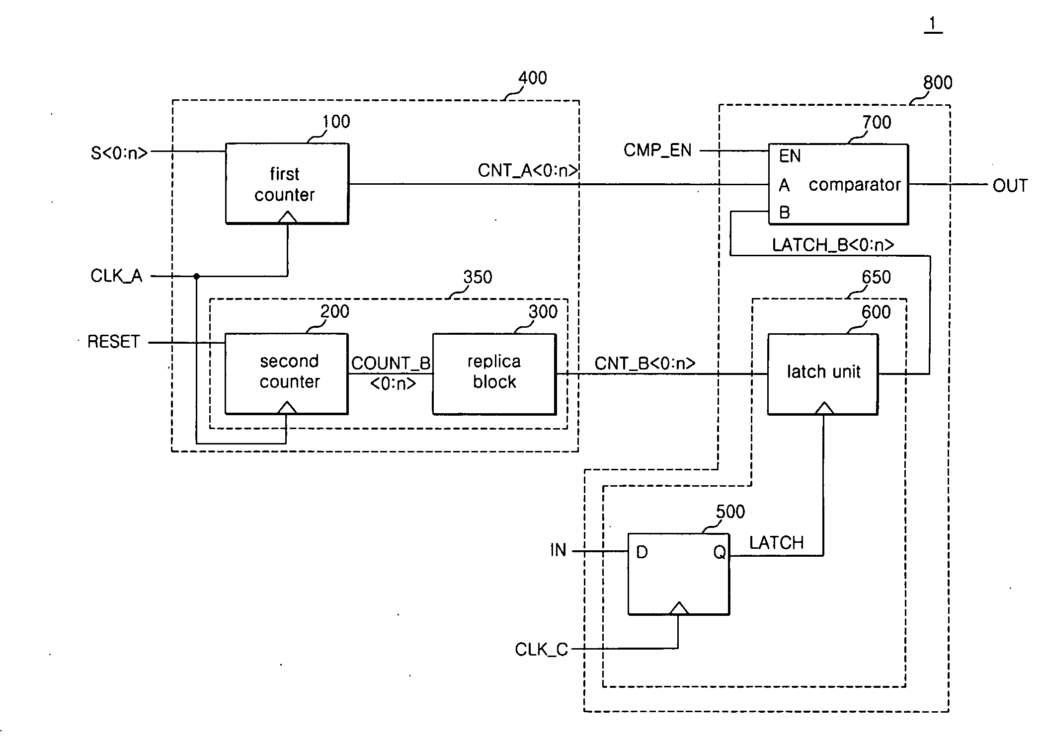
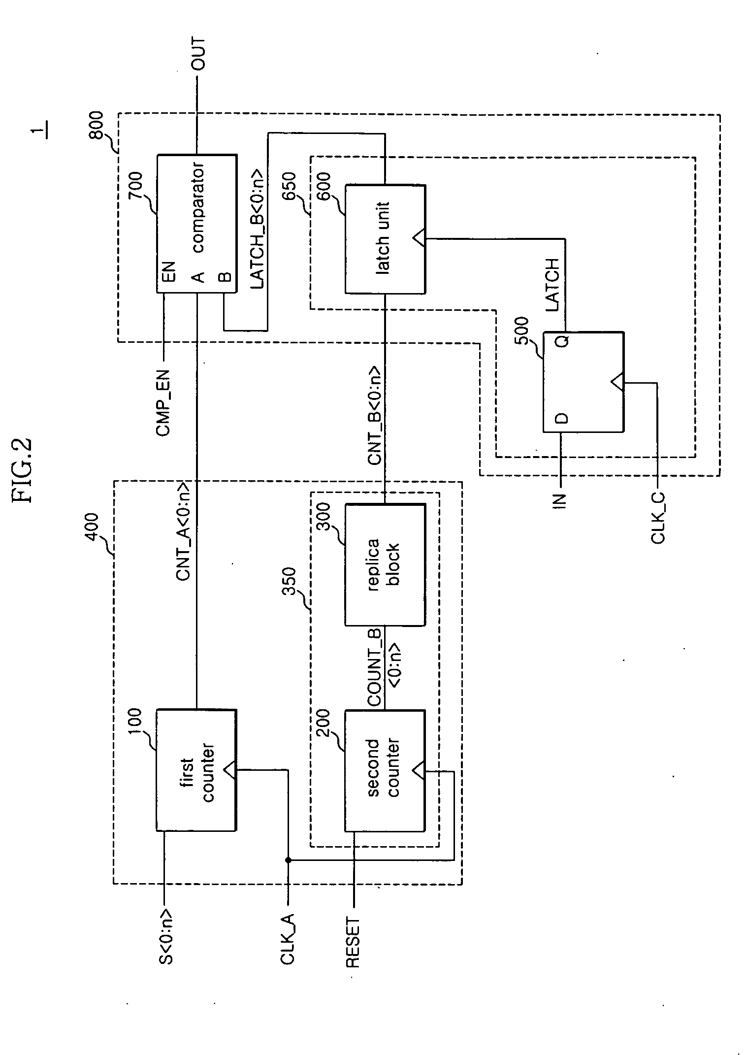
[0031]FIG. 2 is a schematic block diagram of an exemplary domain crossing circuit 1 of a semiconductor memory apparatus according to one embodiment, and FIG. 3 is a schematic block diagram of an exemplary replica block 300 capable of being implemented in the circuit 1 of FIG. 2 according to one embodiment.

[0032]In FIG. 2, the domain crossing circuit 1 can be configured to include a first comparative signal providing unit 400 and a data processing unit 800. The first comparative signal providing unit 400 can include a first counter 100 that is a source counter and a target counter block 350. In addition, the data processing unit 800 can be configured to include a data input unit 500, a latch unit 600, and a comparator 700.

[0033]In FIG. 2, the domain crossing circuit 1 can employ an internal clock signal ‘CLK_A’ which can be substantially the same source clock signal for the first counter 100 and a second counter 200, so that the first and second counters 100 and 200 can simultaneousl...


PUM


Abstract

A domain crossing circuit of a semiconductor memory apparatus, the domain crossing circuit comprising first and second count signals generated at substantially a same clock period, and representing predetermined clock differences with reference to an internal clock signal with respect to same bit combination data, and a data processing unit configured to provide output data corresponding to input data based on the second count signal in response to the input data synchronized to an external clock signal.

Description

CROSS-REFERENCES TO RELATED APPLICATION[0001]The present application claims priority under 35 U.S.C. § 119(a) to Korean application number 10-2008-0087783, filed on Sep. 5, 2008, in the Korean Intellectual Property Office, which is incorporated herein by reference in its entirety as if set forth in full.BACKGROUND[0002]1. Technical Field[0003]The embodiments described herein relate to a semiconductor memory apparatus and more particularly, to a domain crossing circuit of a semiconductor memory apparatus.[0004]2. Related Art[0005]Generally, a synchronous semiconductor memory apparatus operates in synchronization with a clock signal. In this case, command signals or data that have been synchronized with an external clock signal, must be synchronized with an internal clock signal to operate in an internal circuit. In addition, internal clock signals, which have been synchronized with the internal clock signal, must be synchronized with an external clock signal, called “domain crossing”...

Claims


Application Information

Patent Timeline
Patent Type & Authority Applications(United States)
IPC IPC(8): G06F1/12
CPCG06F1/12G11C7/222G11C7/1072G11C7/1051G11C7/10G11C7/22
Inventor CHOI, HAE RANGKIM, YONG JUHAN, SUNG WOOSONG, HEE WOONGOH, IC SUKIM, HYUNG SOOHWANG, TAE JINLEE, JI WANGJANG, JAE MINPARK, CHANG KUN
Owner SK HYNIX INC
Why Eureka
Try Eureka