Nonvolatile semiconductor memory device and method of manufacturing the same

a non-volatile, semiconductor technology, applied in the direction of semiconductor devices, basic electric elements, electrical equipment, etc., can solve the problems of increasing the cost and technology of lithographic processes, physical limitations such as those of withstanding voltage between elements, and the difficulty of miniaturization in terms of cost and technology

Inactive Publication Date: 2010-03-25
KK TOSHIBA
View PDF17 Cites 78 Cited by
  • Summary
  • Abstract
  • Description
  • Claims
  • Application Information

AI Technical Summary

Benefits of technology

[0009]In accordance with a first aspect of the present invention, a nonvolatile semiconductor memory device includes: a plurality of memory strings, each of which has a plurality of electrically rewritable memory cells connected in series; and select transistors, one of which is connected to each of ends of each of the memory strings, each of the memory strings comprising: a first semiconductor layer having a pair of columnar portions extending in a perpendicular direction with respect to a substrate, and a joining portion formed so as to join lower ends of the pair of columnar portions; a charge

Problems solved by technology

However, in recent years, even this miniaturization is becoming difficult in terms of cost and technology.
Improvements in photolithographic technology are necessary for miniaturization, but costs required for lithographic processes are steadily increasing.
Moreover, even if mini

Method used


Image

  • Nonvolatile semiconductor memory device and method of manufacturing the same
  • Nonvolatile semiconductor memory device and method of manufacturing the same
  • Nonvolatile semiconductor memory device and method of manufacturing the same

Examples


first embodiment

[0058](Configuration of a Nonvolatile Semiconductor Memory Device 100 in Accordance with a First Embodiment)

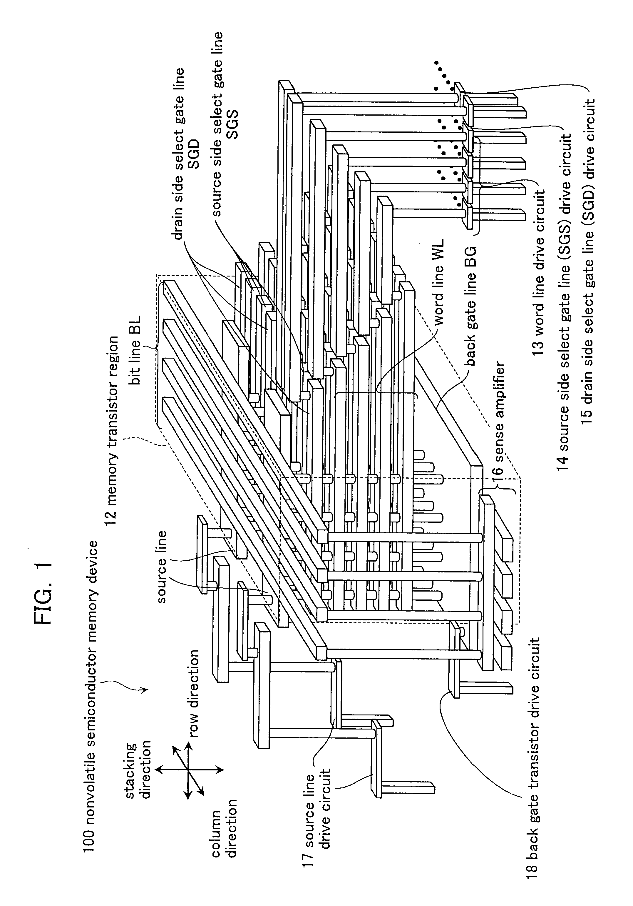
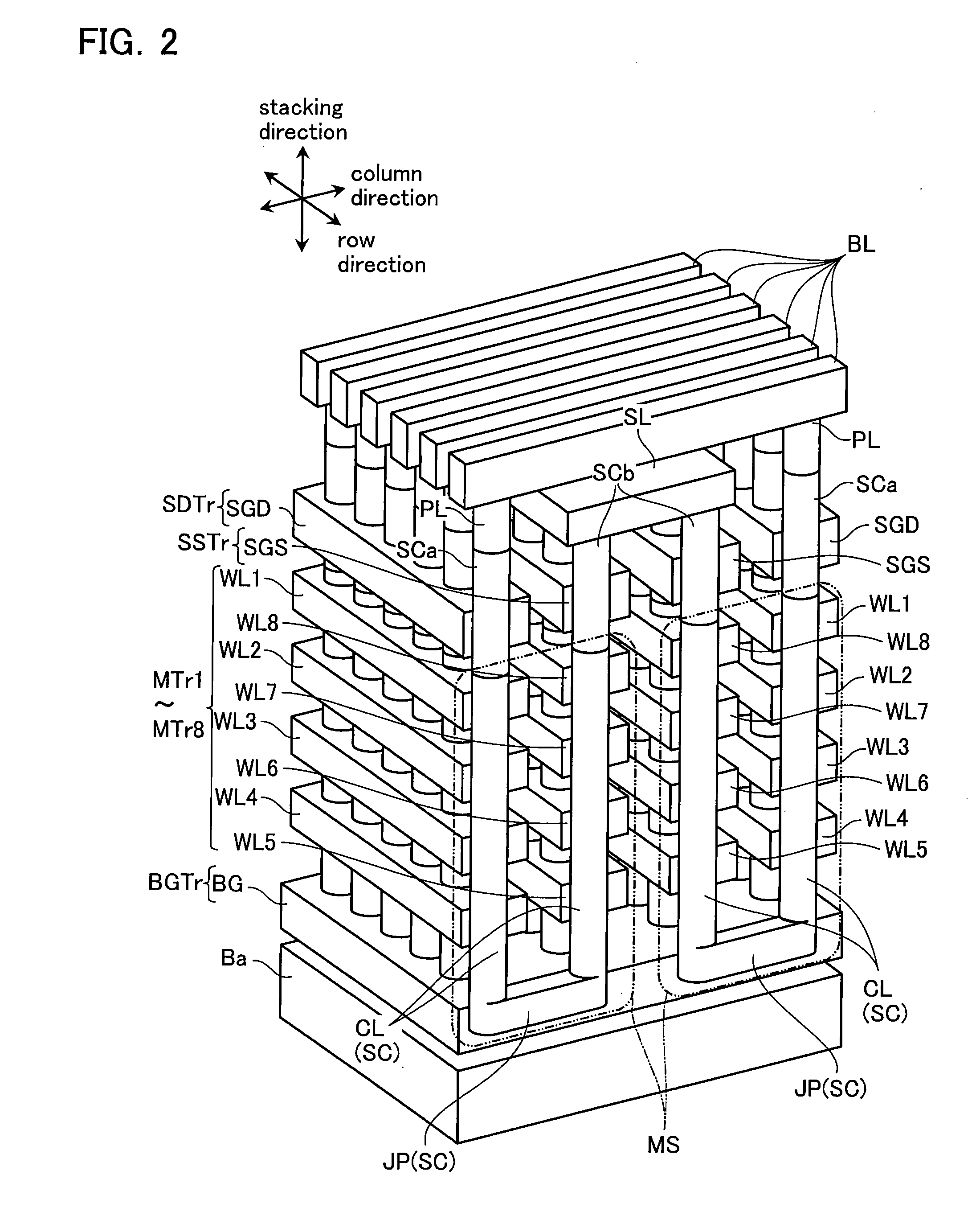
[0059]FIG. 1 shows a schematic view of a nonvolatile semiconductor memory device 100 in accordance with a first embodiment of the present invention. As shown in FIG. 1, the nonvolatile semiconductor memory device 100 in accordance with the first embodiment mainly includes a memory transistor region 12, a word line drive circuit 13, a source side select gate line (SGS) drive circuit 14, a drain side select gate line (SGD) drive circuit 15, a sense amplifier 16, a source line drive circuit 17, and a back gate transistor drive circuit 18. The memory transistor region 12 includes memory transistors configured to store data. The word line drive circuit 13 controls a voltage applied to word lines WL. The source side select gate line (SGS) drive circuit 14 controls a voltage applied to a source side select gate line (SGS). The drain side select gate line (SGD) drive circuit 15 contro...

second embodiment

[0134](Specific Configuration of a Nonvolatile Semiconductor Memory Device in Accordance with a Second Embodiment)

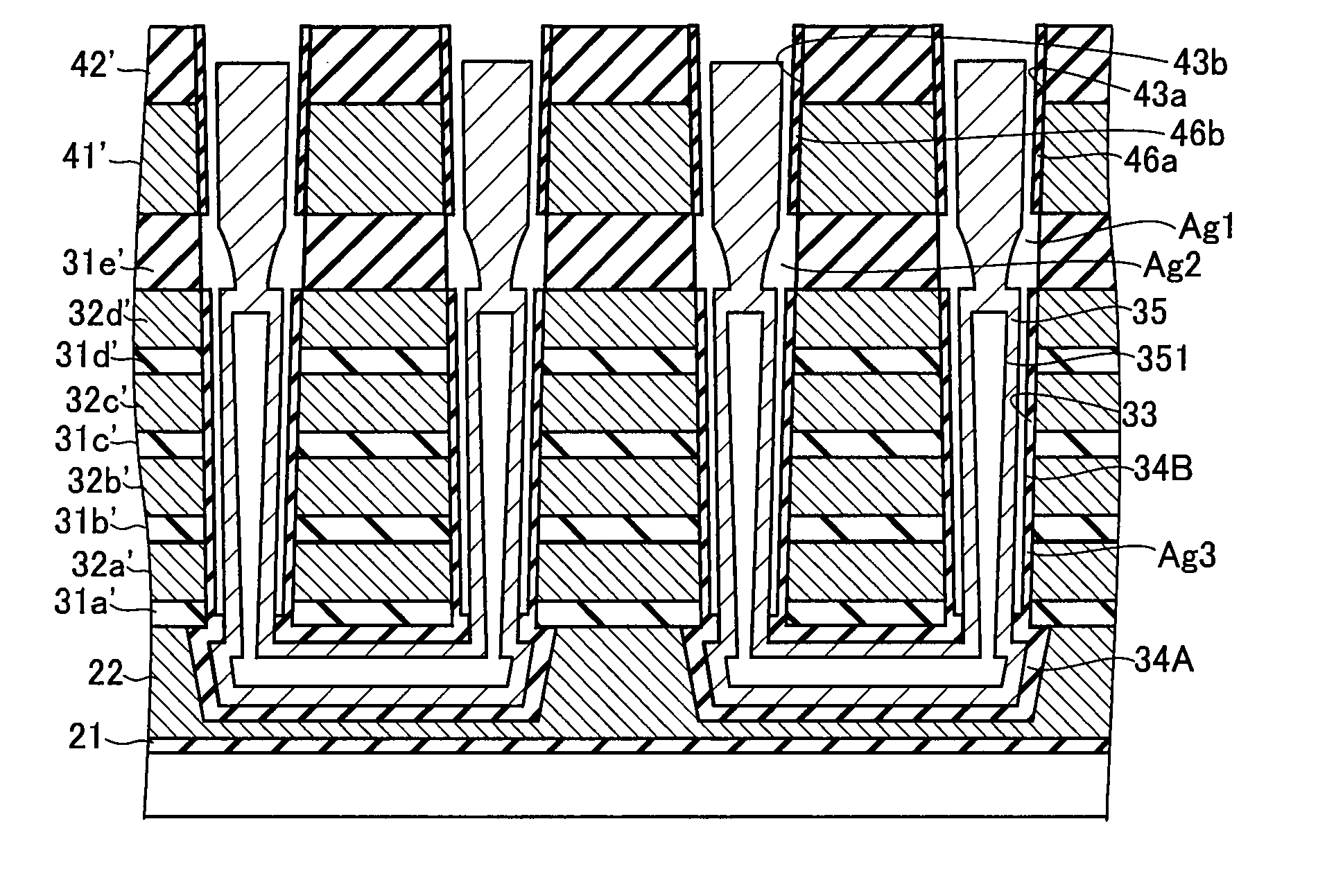
[0135]Next, a specific configuration of a nonvolatile semiconductor memory device in accordance with a second embodiment is described with reference to FIG. 19. FIG. 19 is an enlarged cross-sectional view of a memory transistor region 12 of the nonvolatile semiconductor memory device in accordance with the second embodiment. Note that in the second embodiment, identical symbols are assigned to configurations similar to those in the first embodiment and descriptions thereof are omitted.

[0136]As shown in FIG. 19, the nonvolatile semiconductor memory device in accordance with the second embodiment differs from the first embodiment in that it further includes a first drain side gate insulating layer 46a in a side wall of the drain side conductive layer 41a facing the gap Ag1. In addition, the nonvolatile semiconductor memory device in accordance with the second embodiment di...

third embodiment

[0142](Specific Configuration of a Nonvolatile Semiconductor Memory Device in Accordance with a Third Embodiment)

[0143]Next, a specific configuration of a nonvolatile semiconductor memory device in accordance with a third embodiment is described with reference to FIG. 20. FIG. 20 is an enlarged cross-sectional view of a memory transistor region 12 of the nonvolatile semiconductor memory device in accordance with the third embodiment. Note that in the third embodiment, identical symbols are assigned to configurations similar to those in the first and second embodiments and descriptions thereof are omitted.

[0144]As shown in FIG. 20, the nonvolatile semiconductor memory device in accordance with the third embodiment further includes, in addition to the configuration according to the second embodiment, a second drain side gate insulating layer 47a in a side wall of the drain side columnar semiconductor layer 44a facing the gap Ag1. Moreover, the nonvolatile semiconductor memory device i...


PUM


Abstract

A nonvolatile semiconductor memory device includes a plurality of memory strings, each of which has a plurality of electrically rewritable memory cells connected in series; and select transistors, one of which is connected to each of ends of each of the memory strings. Each of the memory strings is provided with a first semiconductor layer having a pair of columnar portions extending in a perpendicular direction with respect to a substrate, and a joining portion formed so as to join lower ends of the pair of columnar portions; a charge storage layer formed so as to surround a side surface of the columnar portions; and a first conductive layer formed so as to surround the side surface of the columnar portions and the charge storage layer, and configured to function as a control electrode of the memory cells. Each of the select transistors is provided with a second semiconductor layer extending upwardly from an upper surface of the columnar portions; and a second conductive layer formed so as to surround a side surface of the second semiconductor layer with a gap interposed, and configured to function as a control electrode of the select transistors.

Description

CROSS REFERENCE TO RELATED APPLICATIONS[0001]This application is based upon and claims the benefit of priority from prior Japanese Patent Application No. 2008-245070, filed on Sep. 25, 2008, the entire contents of which are incorporated herein by reference.BACKGROUND OF THE INVENTION[0002]1. Field of the Invention[0003]The present invention relates to an electrically rewritable nonvolatile semiconductor memory device and a method of manufacturing the same.[0004]2. Description of the Related Art[0005]Conventionally, an LSI is formed by integrating elements in a two-dimensional plane on a silicon substrate. It is common practice to increase a storage capacity of memory by reducing dimensions of (miniaturizing) an element. However, in recent years, even this miniaturization is becoming difficult in terms of cost and technology. Improvements in photolithographic technology are necessary for miniaturization, but costs required for lithographic processes are steadily increasing. Moreover,...

Claims


Application Information

Patent Timeline
IPC IPC(8): H01L27/115H01L21/8246
CPCH01L27/11578H01L27/11582H01L29/7926H01L29/792H01L29/66833H10B43/20H10B43/27H01L27/0688
Inventor KITO, MASARUFUKUZUMI, YOSHIAKIKATSUMATA, RYOTAKIDOH, MASARUTANAKA, HIROYASUISHIDUKI, MEGUMIKOMORI, YOSUKEAOCHI, HIDEAKI
Owner KK TOSHIBA
Why Eureka
Try Eureka