

On-Chip RF Shields with Backside Redistribution Lines
a technology of rf shields and backside redistribution lines, applied in the field of electronic devices, can solve the problems of rf circuits operating at high frequencies producing extraneous electromagnetic radiation, creating additional challenges that need to be overcome, and affecting the operation of rf shields
- Summary
- Abstract
- Description
- Claims
- Application Information
AI Technical Summary
Benefits of technology
Problems solved by technology
Method used
Image

Examples
Embodiment Construction
[0019]The making and using of the presently preferred embodiments are discussed in detail below. It should be appreciated, however, that the present invention provides many applicable inventive concepts that can be embodied in a wide variety of specific contexts. The specific embodiments discussed are merely illustrative of specific ways to make and use the invention, and do not limit the scope of the invention.
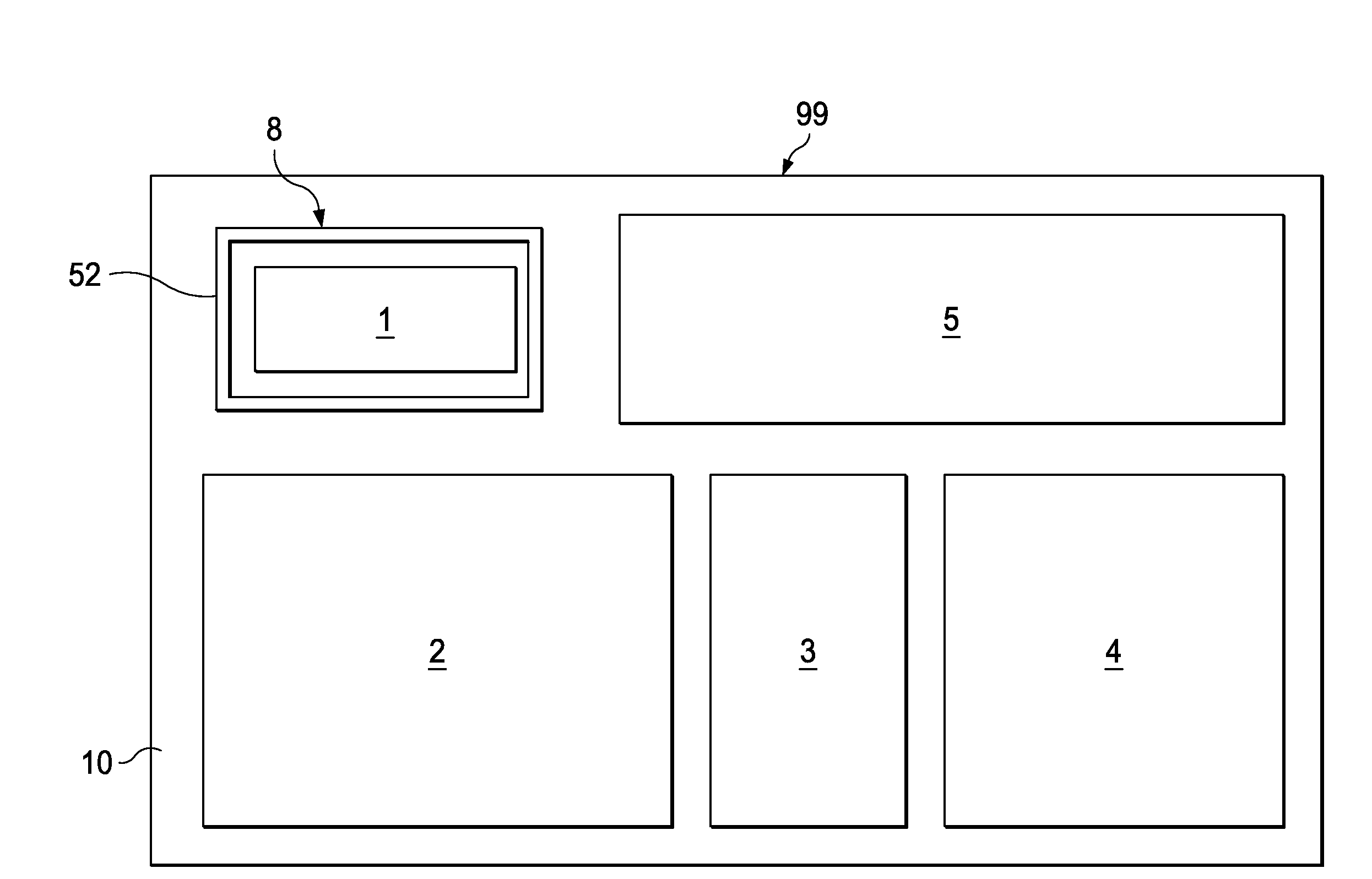
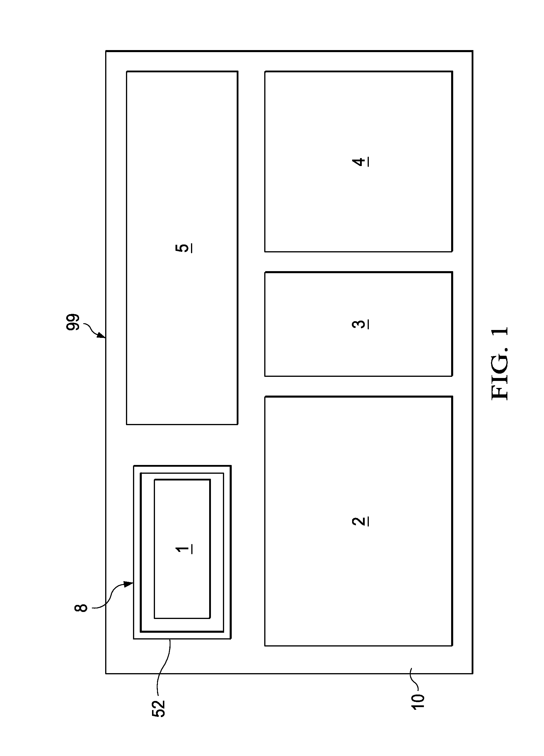
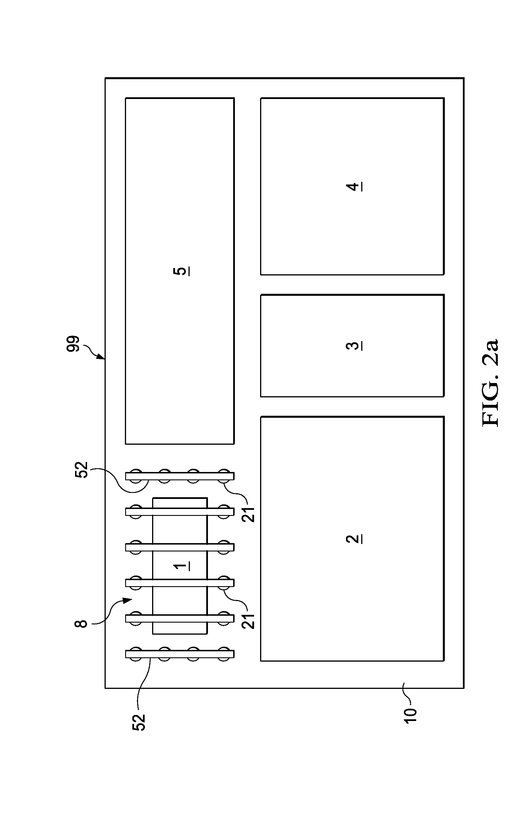
[0020]The present invention will be described with respect to preferred embodiments in a specific context, namely, a structure comprising redistribution lines forming an RF shield. In various embodiments, the invention avoids the use of separate shielding layers or structures outside the chip (for example, additional packaging layers). The present invention avoids expensive fabrication costs by integrating the RF shield on-chip rather than being separately attached to the chip. Further, being an integrated RF shield, the manufacturing steps are commonly shared with other comp...
PUM
 Abstract
Description
Claims
Application Information