MEMS 2d and 3D magnetic field sensors and associated manufacturing method

a magnetic field sensor and manufacturing method technology, applied in the field of hall effect-based devices, can solve the problems of complex measuring protocols, difficult to realize two-dimensional (2d) and three-dimensional (3d) hall probes simple mems processes, and need for adjustment and interconnection of subunits

Active Publication Date: 2010-04-22
JUNIVERSITI OF NORT KAROLINA EHT SHARLOTT
View PDF2 Cites 29 Cited by
  • Summary
  • Abstract
  • Description
  • Claims
  • Application Information

AI Technical Summary

Benefits of technology

[0010]In various exemplary embodiments, the present invention provides Hall effect device configurations capable of measuring magnetic fields in 2D and 3D along with associated MEMS manufacturing methods. The present invention includes various geometric layout configurations for 2D and 3D Hall effect devices with multidimensional magnetic field sensing elements. Advantageously, the present invention can provide, simultaneously and independently, absolute measurement of each of the components (i.e., x-, y-, and z-components) of a magnetic field. Additionally, the geometric layout configurations enable the Hall effect devices to be constructed using various MEMS fabrication techniques.

Problems solved by technology

However, it is difficult to realize two-dimensional (2D) and three-dimensional (3D) Hall probes simple MEMS processes.
These existing protocols / methods have several drawbacks including the need for adjustment and interconnection of the subunits, cross-sensitivity, complicated measuring protocols, as well as the fact that the three magnetic field components are not measured at the same point for 3D units.

Method used


Image

  • MEMS 2d and 3D magnetic field sensors and associated manufacturing method
  • MEMS 2d and 3D magnetic field sensors and associated manufacturing method
  • MEMS 2d and 3D magnetic field sensors and associated manufacturing method

Examples


Embodiment Construction

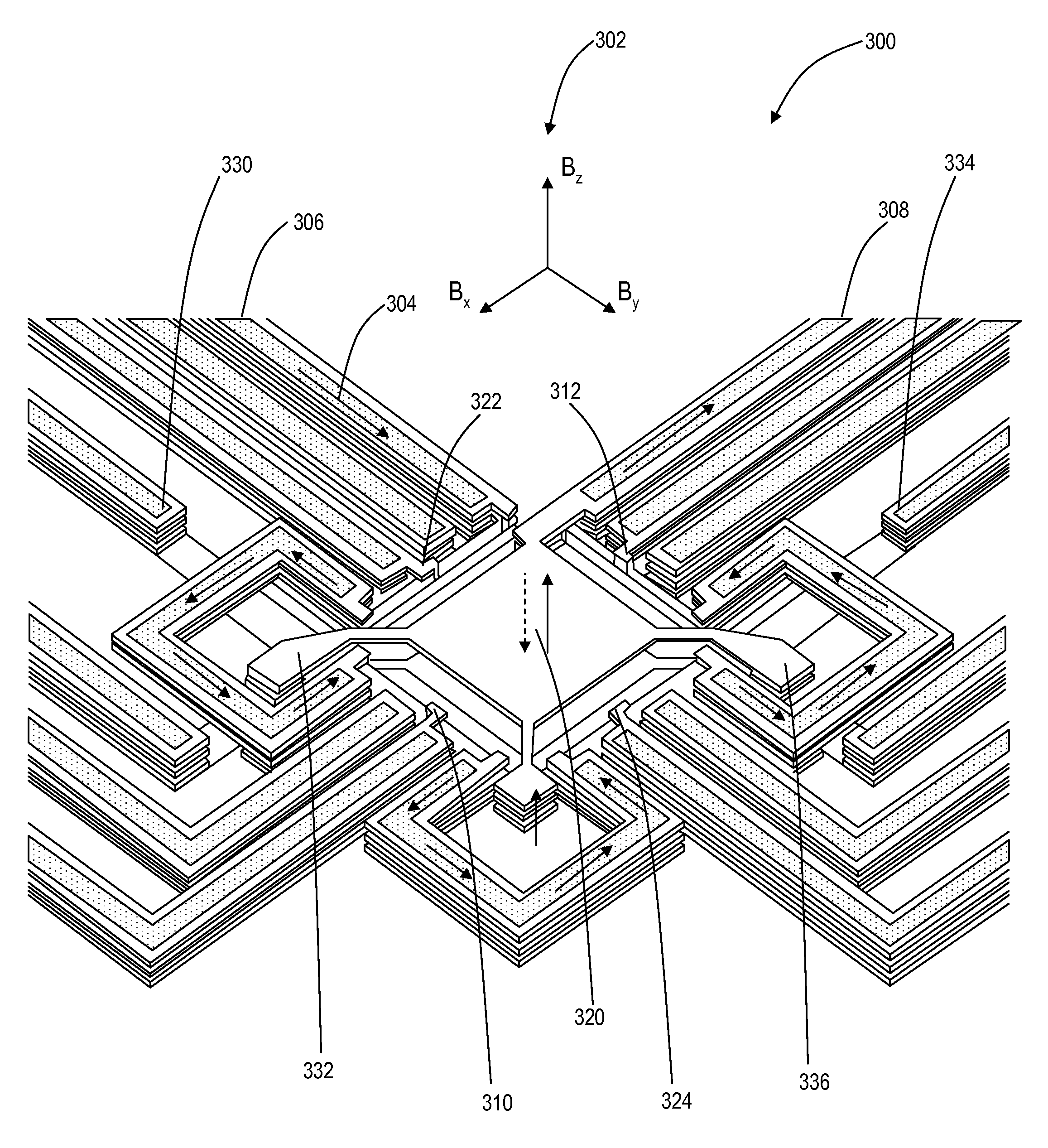
[0032]In various exemplary embodiments, the present invention provides Hall effect device configurations capable of measuring magnetic fields in 2D and 3D along with associated MEMS manufacturing methods. The present invention includes various geometric layout configurations for 2D and 3D Hall effect devices with multidimensional magnetic field sensing elements. Advantageously, the present invention can provide, simultaneously and independently, absolute measurement of each of the components (i.e., x-, y-, and z-components) of a magnetic field. Additionally, the geometric layout configurations enable the Hall effect devices to be constructed with MEMS fabrication techniques.

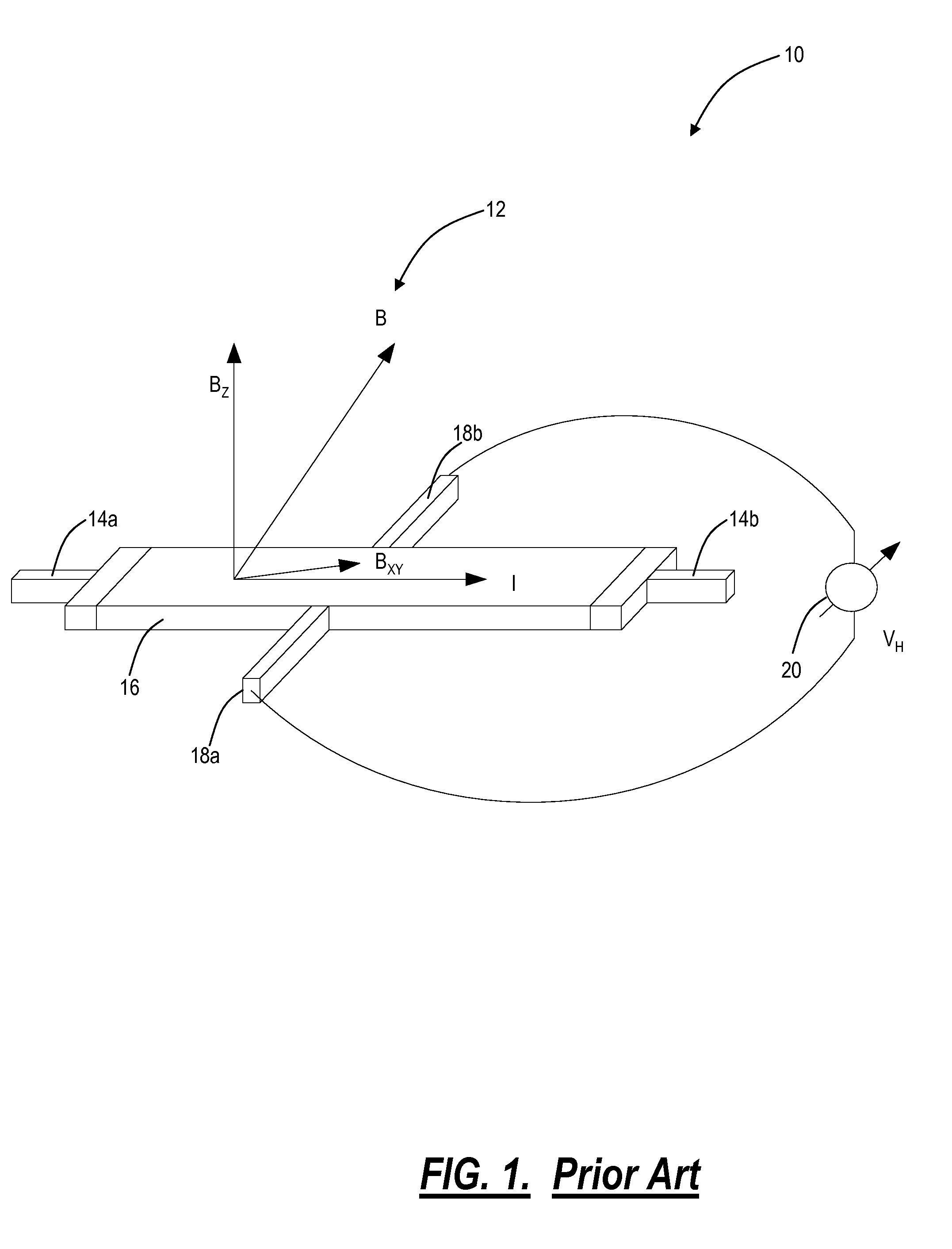
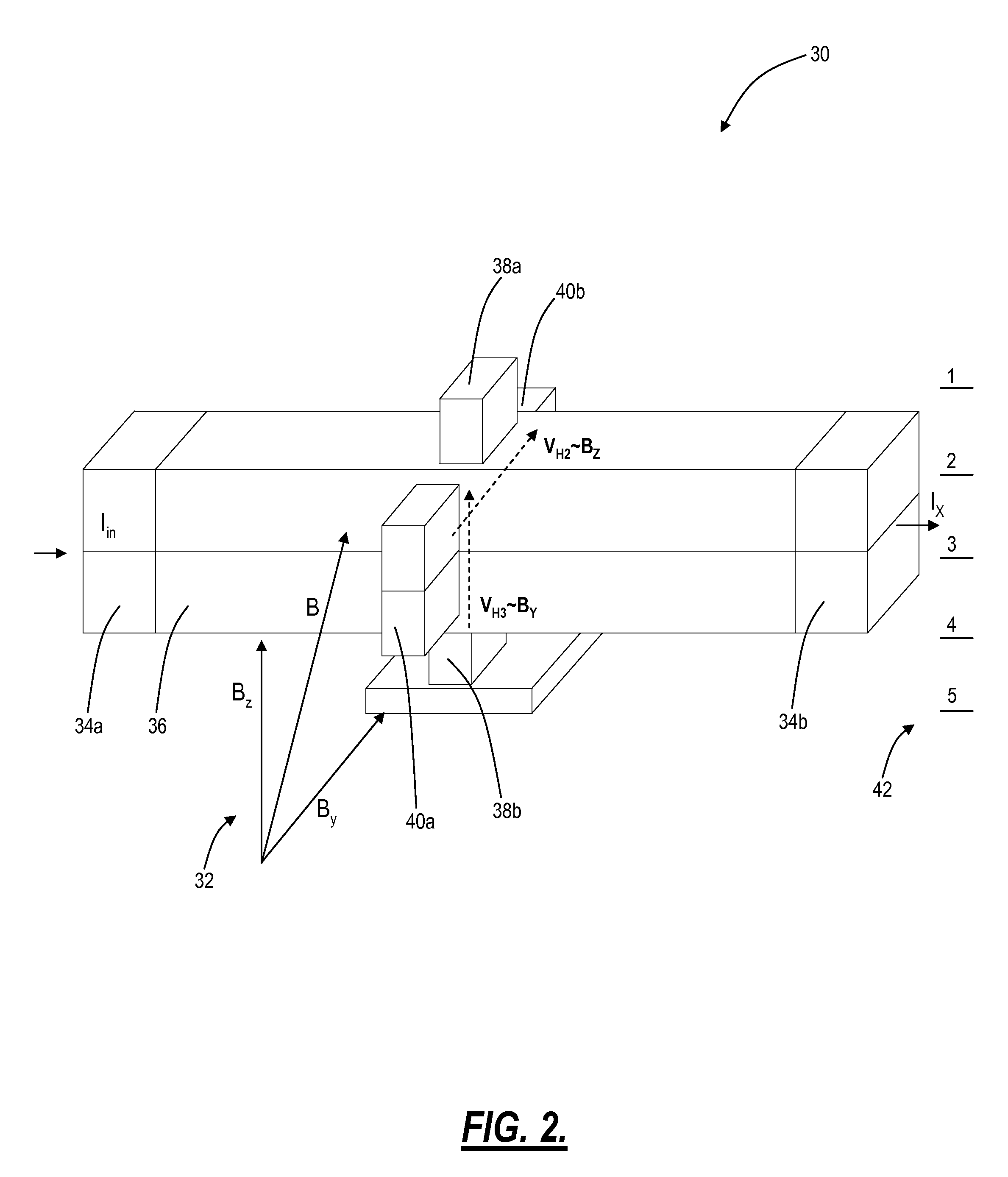
[0033]In an exemplary embodiment, the Hall probe configuration can be either: (a) a cube, rectangular parallelepiped, parallelogram, or the like of polysilicon material, mono-crystalline material, or the like, or (b) a set of multiple plates, orthogonally positioned in space but separated from each other (box), i...


PUM


Abstract

The disclosure provides Hall effect device configurations capable of measuring magnetic fields in two dimensions (2D) and three dimensions (3D) along with associated microelectromechanical system (MEMS) manufacturing methods. The present invention includes various geometric layout configurations for 2D and 3D Hall effect devices with multidimensional magnetic field sensing elements. Advantageously, the present invention can provide, simultaneously and independently, absolute measurement of each of the components (i.e., x-, y-, and z-components) of a magnetic field. Additionally, the geometric layout configurations enable the Hall effect devices to be constructed with MEMS fabrication techniques.

Description

FIELD OF THE INVENTION[0001]The present invention relates generally to Hall effect-based devices. More specifically, the present invention provides multidimensional magnetic field sensing elements with Hall effect device configurations capable of measuring magnetic fields in two-dimensions (2D) and three-dimensions (3D) along with associated microelectromechanical system (MEMS) manufacturing methods.BACKGROUND OF THE INVENTION[0002]A Hall probe (also known as a Hall sensor) is a semiconductor-based detector which uses the Hall effect to measure the strength of a magnetic field. The probe provides an output voltage proportional to the magnitude of a magnetic field. In a conductive material, moving electrical charges (i.e., an electrical current) are affected by a nearby magnetic field. Bending (Lorentz) forces are experienced by the moving charges, which can be described by:Fq=q·vq×B=q·|vq|×|B|·sin(θ)[0003]The result is what may be seen as an orthogonal charge drift, with a build up ...

Claims


Application Information

Patent Timeline
Patent Type & Authority Applications(United States)
IPC IPC(8): G01R33/07H01L21/02
CPCG01R33/0005G01R33/0206H01L43/065G01R33/07G01R33/0286H10N52/101
Inventor ESTRADA, HORACIO V.MAKSYMIV, YAROSLAV
Owner JUNIVERSITI OF NORT KAROLINA EHT SHARLOTT
Why Eureka
Try Eureka