Exposure apparatus and device manufacturing method

a technology of exposure apparatus and manufacturing method, which is applied in the direction of measuring devices, printing, instruments, etc., can solve the problems of error, index mark imaging position deviating from the designed position, and worse exposure performan

Inactive Publication Date: 2010-04-22
CANON KK
View PDF9 Cites 6 Cited by
  • Summary
  • Abstract
  • Description
  • Claims
  • Application Information

AI Technical Summary

Problems solved by technology

If the base line amount changes, when the wafer W is moved below the projection optical system PO after the alignment mark is measured with the alignment detection system OA, an error is caused.
Further, the imaging position of the index mark may deviate from the designed position because of aberration remaining in the optical system of the focus detection system FS and an installation error of the focus detection system FS.
This may worsen exposure performance.

Method used


Image

  • Exposure apparatus and device manufacturing method
  • Exposure apparatus and device manufacturing method
  • Exposure apparatus and device manufacturing method

Examples


first embodiment

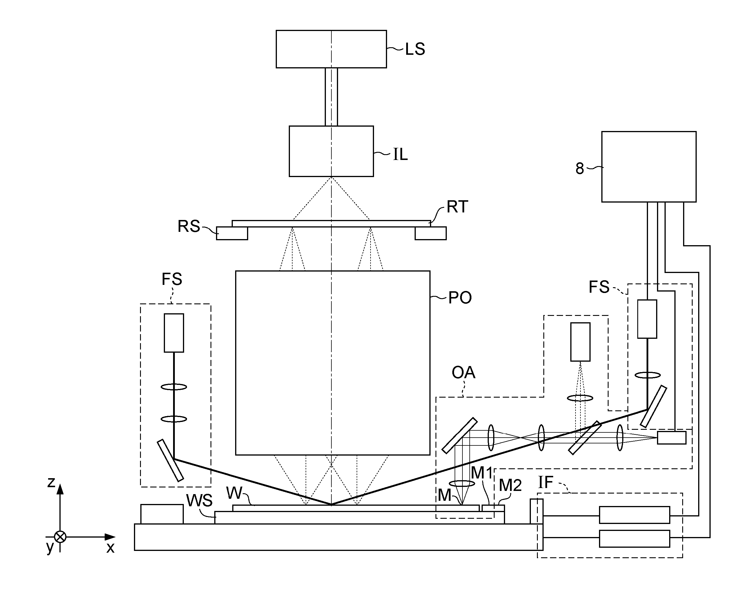
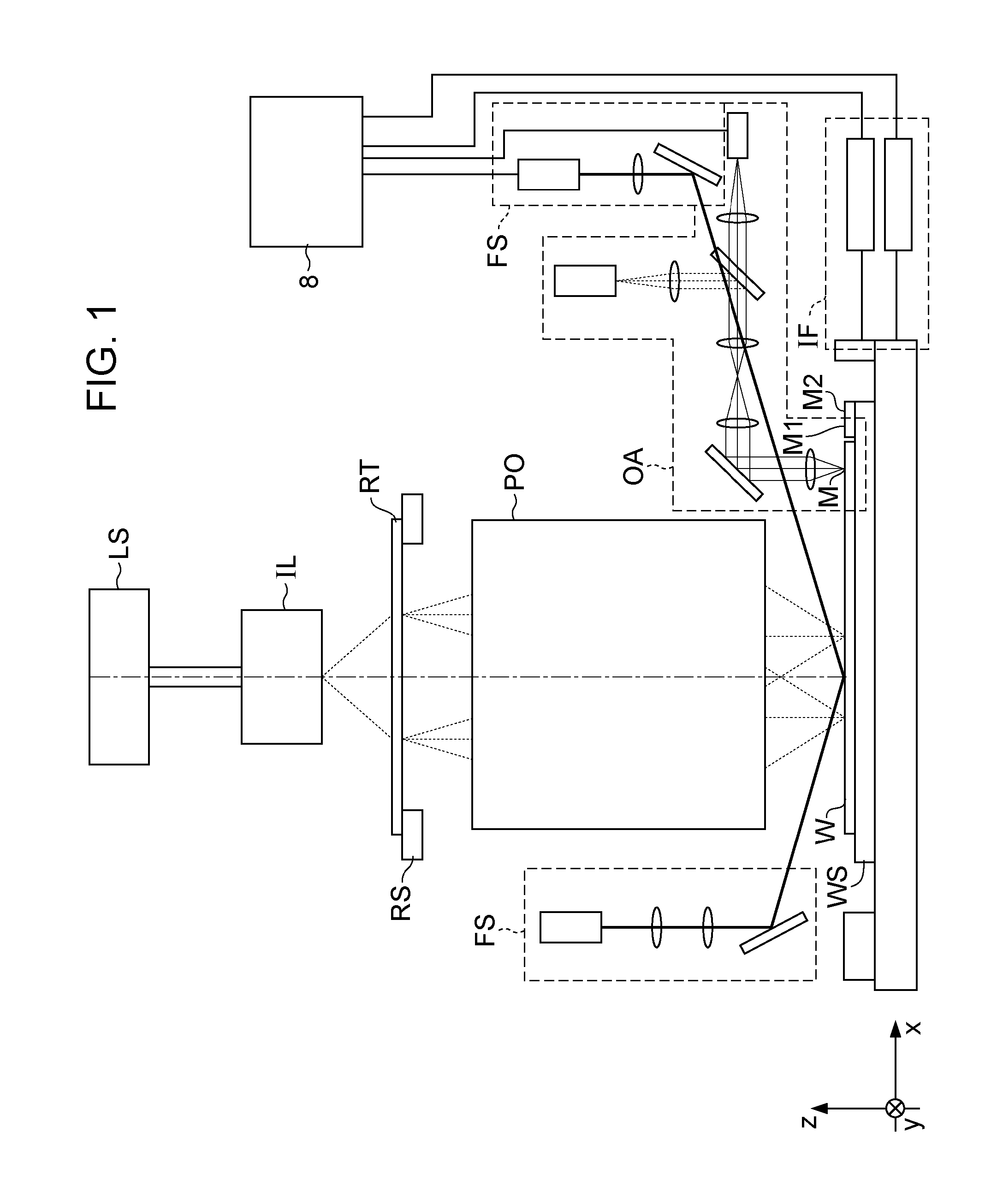
[0033]An exposure apparatus according to the present invention will be described below with reference to FIG. 1.

[0034]The exposure apparatus of the first embodiment projects a circuit pattern of a reticle RT onto a wafer W mounted on a wafer stage WS by exposure via a projection optical system PO.

[0035]A light source LS is a KrF excimer laser or an ArF excimer laser, and emits ultraviolet light. A reticle stage RS moves a reticle (original) RT, and a wafer stage WS moves a wafer (substrate) W. An illumination optical system IL illuminates the reticle RT with ultraviolet light emitted from the light source LS. A projection optical system PO projects a pattern image of the reticle RT onto the wafer W.

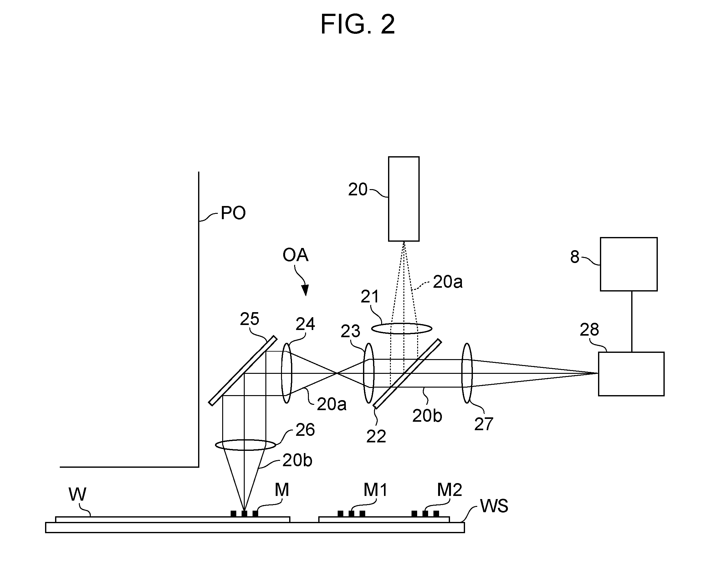
[0036]An alignment detection system OA is provided outside the optical axis of the projection optical system PO. The alignment detection system OA optically detects an alignment mark M provided on the wafer W, and measures the position of the wafer W. In the first embodiment, the alignmen...

second embodiment

[0056]Next, the present invention will be described with reference to FIGS. 7A and 7B.

[0057]In the first embodiment, the height in the z-direction of the image of the index mark M3 is first measured, and the position in the xy-direction of the image of the index mark M3 is then found. In contrast, in the second embodiment, the positions in the x-, y-, and z-directions of the image of the index mark M3 are found simultaneously. The configuration of an exposure apparatus of the second embodiment is similar to that adopted in the first embodiment.

[0058]In the second embodiment, the intensity of detection light is first acquired while driving a wafer stage WS in the x-direction (or y-direction) at a predetermined height in the z-direction.

[0059]Next, an alignment-detection-system measurement mark M1 and a focus-detection-system measurement mark M2 are slightly moved in the z-direction, and the intensity of detection light is acquired while moving the marks in the x-direction (or y-direc...

third embodiment

[0062]the present invention will now be described.

[0063]When a plurality of wavelengths are used, chromatic aberration is caused by the optical factor of a focus detection system FS, and a projected position of an index mark M3 is displaced. To correct this displacement, the following method is adopted.

[0064]Chromatic aberration due to the wavelengths can be measured by performing measurement with the same exposure apparatus and in the same method as those in the first and second embodiments and detecting a difference between the wavelengths.

[0065]In the third embodiment, the difference is corrected by switching the wavelength of detection light used in the focus detection system FS. That is, displacement of the projected position of the index mark M3 is measured by switching among a plurality of detection light wavelengths used in the focus detection system FS. The measured displacement amount may be corrected by chromatic-aberration correcting optical members 42a and 42b provided ...


PUM


Abstract

An apparatus includes a stage configured to move a substrate, an optical system configured to project an image of a pattern on an original onto the substrate, an alignment detection system configured to detect an image of an alignment mark formed on the substrate and measure a position of the alignment mark, and a focus detection system having an index mark and configured to measure a height of the substrate by projecting an image of the index mark onto the substrate. The stage includes an alignment measurement mark and a focus measurement mark that has a positional relationship with the alignment measurement mark. The alignment detection system measures a position of the alignment measurement mark. The focus detection system measures a position of the image of the index mark by projecting the image of the index mark onto the focus measurement mark.

Description

BACKGROUND OF THE INVENTION[0001]1. Field of the Invention[0002]The present invention relates to an apparatus and a device manufacturing method.[0003]2. Description of the Related Art[0004]To manufacture devices (e.g., a semiconductor integrated circuit device and a liquid crystal display device), an exposure apparatus of a static exposure type, such as a stepper, and an exposure apparatus of a scanning exposure type, such as a step-and-scan exposure apparatus, are used.[0005]FIG. 13 shows the configuration of an exposure apparatus of the related art. An illumination optical system IL illuminates a reticle RT serving as an original with light from an exposure light source LS. The reticle RT is provided with a fine circuit pattern to be transferred. An image of the pattern is projected onto a wafer W by a projection optical system PO.[0006]The projection optical system PO is to have as large a resolving power as possible. To increase the resolving power, the numerical aperture of the...

Claims


Application Information

Patent Timeline
Patent Type & Authority Applications(United States)
IPC IPC(8): G03B27/32G01B11/00G03B27/58
CPCG03B27/32G03F9/7026G03F9/7088G03F9/7084G03F9/7076
Inventor SATO, HIROSHI
Owner CANON KK
Why Eureka
Try Eureka