Semiconductor package

a semiconductor and leadframe technology, applied in the direction of casings/cabinets/drawers, electrical apparatus construction details, etc., can solve the problems of poor bonding strength, moisture, noise or ground coupling of e-pad leadframe packages, etc., to improve the structure of semiconductor packages, reduce ground coupling, and improve performan

Active Publication Date: 2010-05-20
MEDIATEK INC
View PDF11 Cites 14 Cited by
  • Summary
  • Abstract
  • Description
  • Claims
  • Application Information

AI Technical Summary

Benefits of technology

[0009]It is one objective of this invention to provide an improved semiconductor package structure with improved performance and reduced ground coupling.

Problems solved by technology

It has been found that the E-pad leadframe package is subject to attacks of moisture.
However, the prior art leadframe package with such ground bridge bar configuration has a shortcoming of that the analog and digital ground wires randomly bonded together onto the ground bridge bar can result in noise or ground coupling, which is also known as water wave effects in TV systems.
Another shortcoming is that the ground bridge bar is vulnerable to twist and deform, leading to poor bonding strength.

Method used


Image

  • Semiconductor package
  • Semiconductor package
  • Semiconductor package

Examples


Embodiment Construction

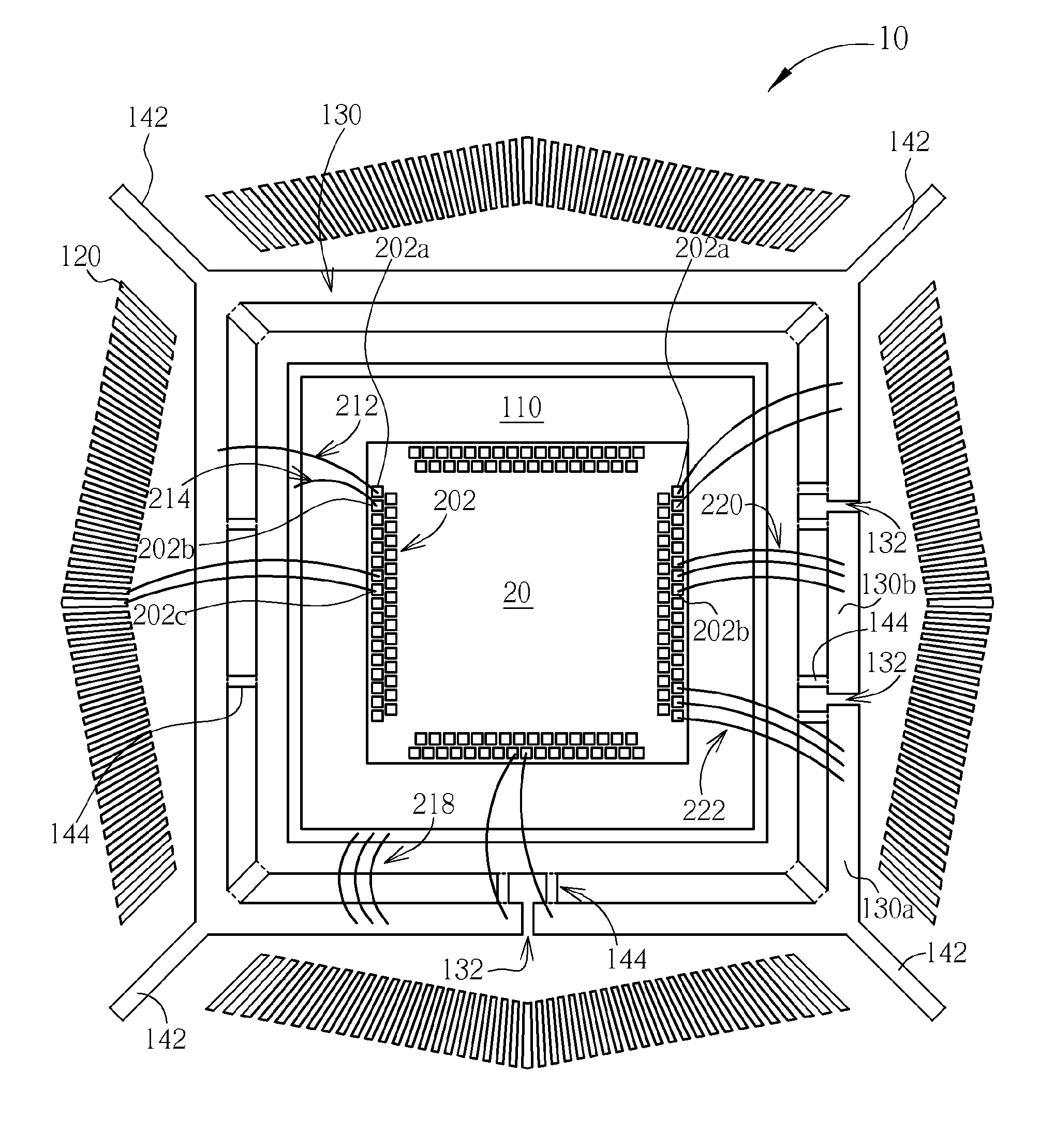
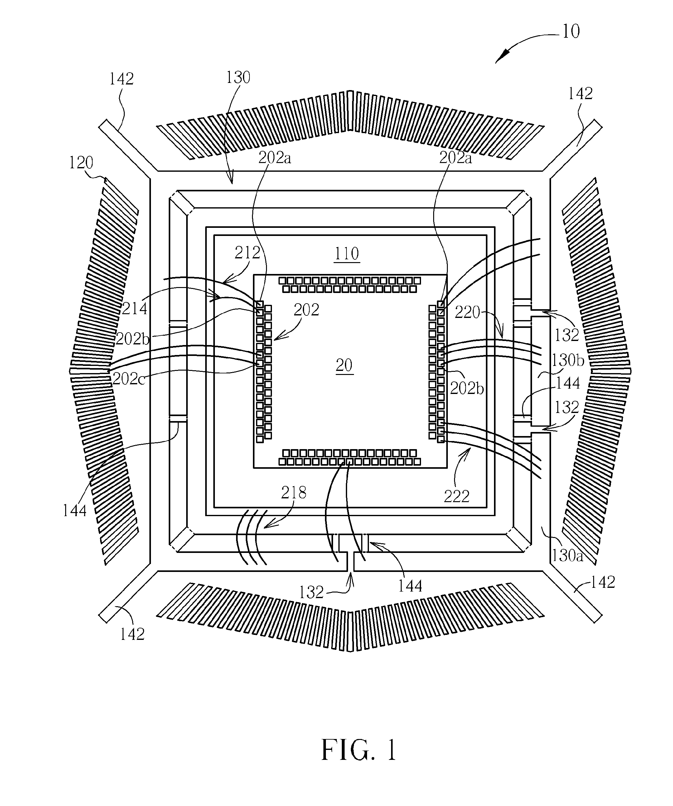
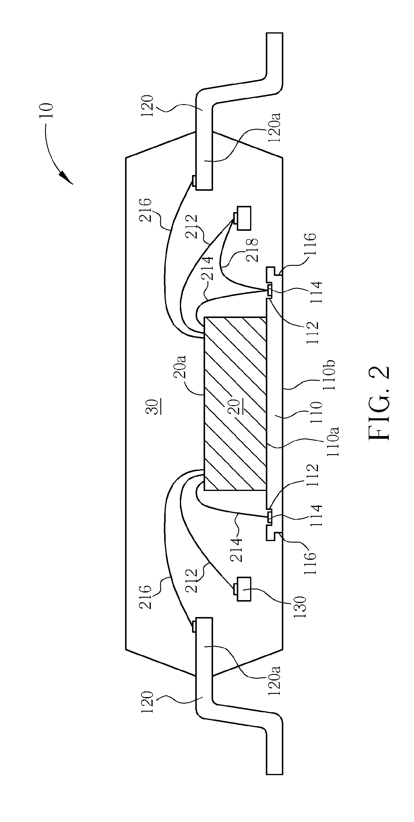
[0019]The technology trend in the consumer electronics can be summarized as more functionalities in a smaller geometry with low cost. The exposed pad low-profile quad flat package (E-pad LQFP) is a low cost solution for multimedia chips, but its disadvantages are limited pin count and worse electrical characteristics.

[0020]As previously mentioned, one problem relates to delamination of the leadframe components from the plastic package body, and the attendant problem of penetration of the package by moisture. In particular, the various parts of a semiconductor package experience greatly different amounts of thermal expansion and contraction with temperature changes due to the relatively large differences in the coefficients of thermal expansion of their respective materials, e.g., metal, epoxy resin, and silicon. As a result, the leadframe components can become delaminated from the package body with temperature cycling of the package during manufacture or operation.

[0021]Where delami...


PUM


Abstract

A semiconductor package includes a die pad; a semiconductor die mounted on the die pad; a plurality of leads in a first horizontal plane disposed along peripheral edges of the die pad; a ground bar downset from the first horizontal plane to a second horizontal plane between the leads and the die pad; a plurality of downset tie bars connecting the ground bar with the die pad; a plurality of ground wires bonding to both of the ground bar and the die pad; and a molding compound at least partially encapsulating the die pad, inner ends of the leads such that bottom surface of the die pad is exposed within the molding compound.

Description

BACKGROUND OF THE INVENTION [0001]1. Field of the Invention[0002]This invention relates generally to packaging of semiconductors, and in particular, to a leadframe semiconductor package.[0003]2. Description of the Prior Art[0004]Leadframe semiconductor packages are well known in the art. A conventional leadframe typically includes a plurality of metal leads temporarily held together in a planar arrangement about a central region during package manufacture by a rectangular frame. A die pad is supported in the central region by a plurality of tie bars that attach to the frame. The leads extend from a first end integral with the frame to an opposite second end adjacent to, but spaced apart from, the die pad.[0005]During package manufacture, a semiconductor die is attached to the die pad. Wire-bonding pads on the die are then connected to selected ones of the inner ends of the leads by fine, conductive bonding wires to convey power, ground or signals between the die and the leads. A pro...

Claims


Application Information

Patent Timeline
Patent Type & Authority Applications(United States)
IPC IPC(8): H01L23/495
CPCH01L2224/48253H01L2224/48247H01L2224/48257H01L24/48H01L2924/01082H01L2924/19107H01L2924/30107H01L23/49503H01L23/49541H01L23/49551H01L24/49H01L2224/48091H01L2924/01006H01L2224/49109H01L2224/4911H01L2224/49113H01L2224/4943H01L2924/01014H01L2924/01033H01L2924/01047H01L2924/01078H01L2924/00014H01L2924/00H01L2924/181H01L2224/05554H01L2924/10162H01L2224/49433H01L2224/45099H01L2224/05599H01L2924/00012
Inventor CHEN, NAN-JANGWONG, YAU-WAI
Owner MEDIATEK INC
Why Eureka
Try Eureka