Image Sensor Module and Method for Manufacturing the Same

Inactive Publication Date: 2007-07-12
ADVANCED SEMICON ENG INC
View PDF3 Cites 17 Cited by
  • Summary
  • Abstract
  • Description
  • Claims
  • Application Information

AI Technical Summary

Benefits of technology

[0005]Accordingly, there is an urgent need to provide an improved package structure of the image sensor module and a method for manufacturing the same, so as to solve the light leakage problem of the image sensor module, thereby achieving the purpose of increased image sensor quality and the process yield.
[0006]An aspect of the present invention provides a package structure of the image sensor module, which has a substrate designed to have a central protrusion that directly fits to a holder of the lens module for positioning, so as to solve the light leakage problem of the image sensor module.
[0007]Another aspect of the present invention provides a method for manufacturing an image sensor module, which detects a center of a sensing region of an optical sensor chip, and then aligns the lens optical axis to the center, so that the lens optical axis of the lens module is substantially situated at the center of the sensing region, thereby greatly increasing the image sensor quality and the process yield.
[0014]With application to the aforementioned package structure of the image sensor module, the substrate is designed to have the central protrusion formed thereon, so that the central protrusion directly fits to the holder of the lens module for positioning, so as to solve the light leakage problem of the image sensor module. In addition, when the package structure of the image sensor module of the present invention is packaging, an aligning process is carried out between a lens optical axis of the lens module and a center of an optical sensor area of the optical sensor chip, so as to ensure the lens optical axis of the lens module being substantially aligned to the center of an optical sensor area of the optical sensor chip, thereby greatly increasing the image sensor quality and the process yield. Hence, in comparison with other prior package structures and packaging processes, the structure and the method disclosed by the present invention are capable of solving the problem of low image sensor quality, and greatly reducing the process time and cost as well.

Problems solved by technology

At this time, if an opaque adhesive material is employed to seal the positioning hole 10a on the lower surface 14 of the substrate 10 completely, it will need to add an additional treatment, and cause the increase of time and cost of package process.

Method used


Image

  • Image Sensor Module and Method for Manufacturing the Same
  • Image Sensor Module and Method for Manufacturing the Same
  • Image Sensor Module and Method for Manufacturing the Same

Examples


Embodiment Construction

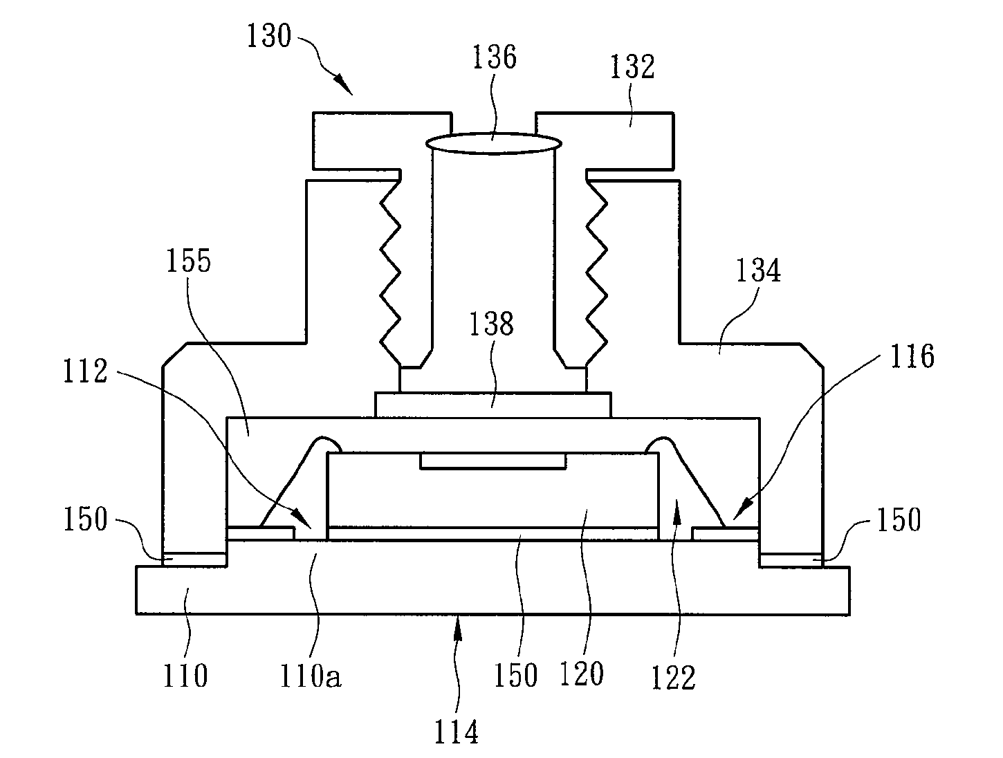
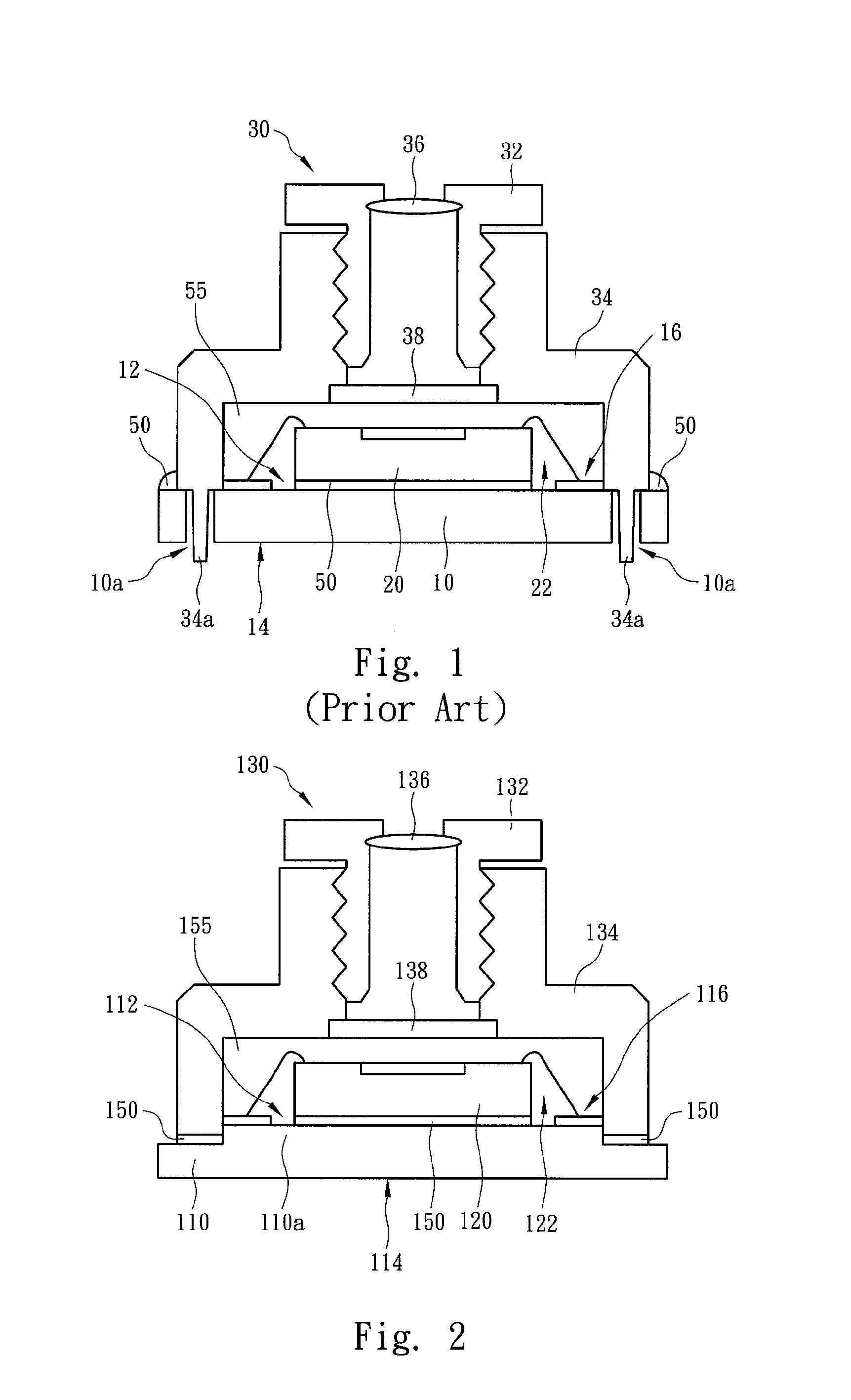
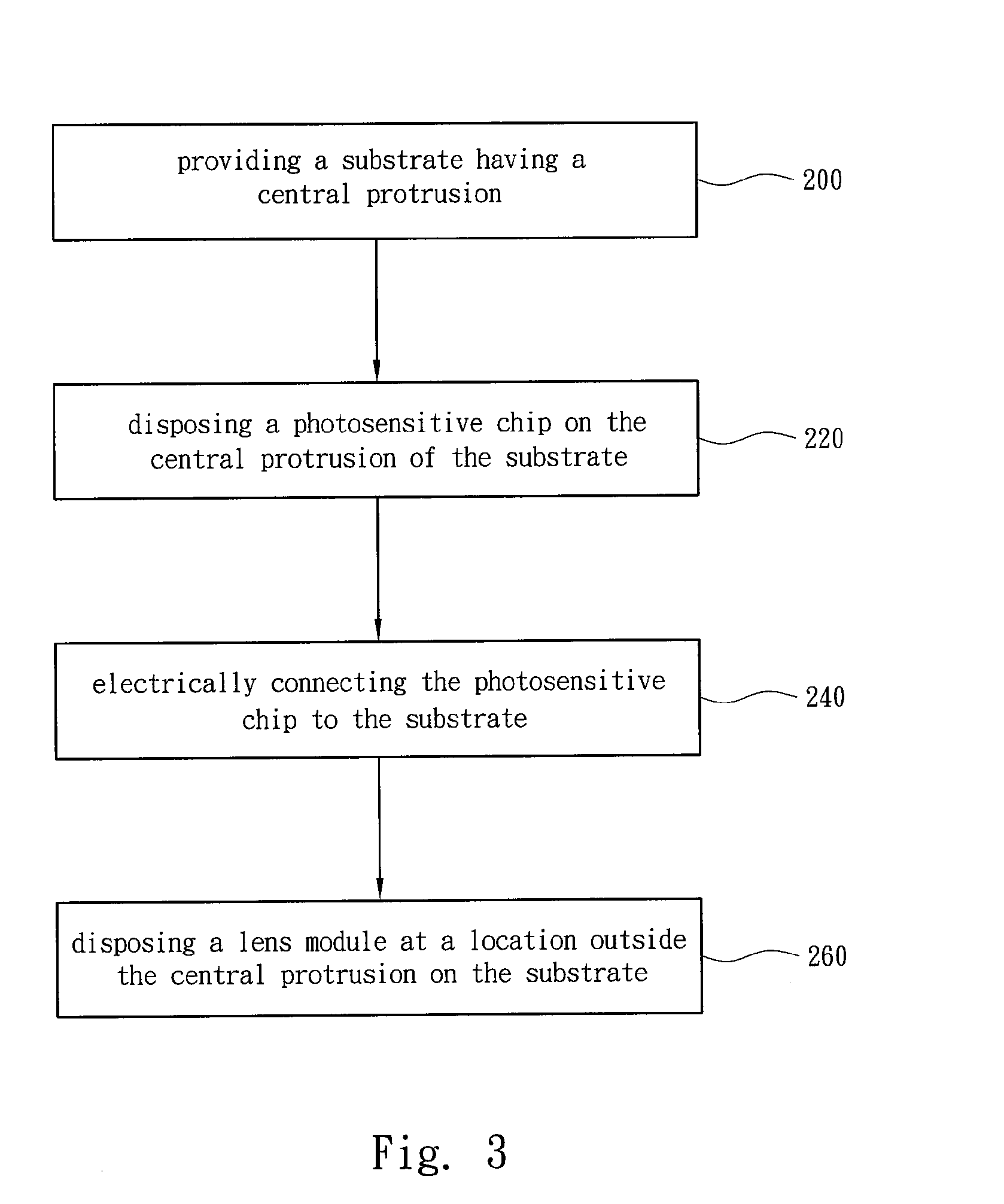
[0019]Reference is made to FIG. 2, which depicts a cross-sectional diagram of a package structure of an image sensor module according to one preferred embodiment of the present invention. The package structure of the image sensor module comprises a substrate 110 having a central protrusion 110a, an optical sensor chip 120 and a lens module 130. In this embodiment, the substrate 110 may be a PCB, which has an upper surface 112 and a lower surface 114 opposite to the upper surface 112, wherein the central protrusion 110a is formed on the upper surface 112, and the central protrusion 110a has a plurality of circuit contacts 116 disposed thereon.

[0020]The optical sensor chip 120, for example, a photodiode, a CCD or a phototransistor CMOS sensor device, is disposed on the central protrusion 110a of the substrate 110, wherein the optical sensor chip 120 is electrically connected to the circuit contacts 116 on the central protrusion 110a by way of a plurality of conductive wires 122.

[0021]...


PUM


Abstract

An image sensor module includes a substrate having a central protrusion formed on an upper surface thereof, an optical sensor chip disposed on the central protrusion and electrically coupled to the substrate, and a lens module disposed on the upper surface of substrate at a location outside the central protrusion. The lens module has a cavity for receiving the optical sensor chip. The central protrusion of the substrate fits to the opening of the cavity of the lens module.

Description

RELATED APPLICATIONS[0001]The present application is based on, and claims priority from, Taiwan Application Serial Number 95101086, filed Jan. 11, 2006, the disclosure of which is hereby incorporated by reference herein in its entirety.FIELD OF THE INVENTION[0002]This invention relates generally to an image sensor module and a method for manufacturing the same, and more particularly, to an image sensor module having functions of reducing light leakage and alignment deviation and a method for manufacturing the same.BACKGROUND OF THE INVENTION[0003]Reference is made to FIG. 1, which depicts a cross-sectional diagram of the structure of the prior image sensor module, which mainly includes a substrate 10, an optical sensor chip (i.e. CMOS chip) 20, and a lens module 30. The substrate 10 is a printed circuit board (PCB), which has an upper surface 12 and a lower surface 14 opposite to the upper surface 12, wherein the upper surface 12 has a plurality of circuit contacts 16 disposed there...

Claims


Application Information

Patent Timeline
IPC IPC(8): H01J5/02H01J40/14
CPCH01L27/14618H01L31/0203H01L27/14685H01L27/14625H01L2224/32225H01L2224/48091H01L2224/48227H01L2224/73265H01L2924/00014H01L2924/00
Inventor WANG, SHENG-YUAN
Owner ADVANCED SEMICON ENG INC
Why Eureka
Try Eureka