Array substrate for liquid crystal display device and method of fabricating the same

Inactive Publication Date: 2007-10-11
LG DISPLAY CO LTD
View PDF4 Cites 28 Cited by
  • Summary
  • Abstract
  • Description
  • Claims
  • Application Information

AI Technical Summary

Benefits of technology

[0015]An advantage of the present invention is to provide an array substrate for a liquid crystal display device that includes an improved gate insulating layer and a method of fabricating the array substrate where a process yield is improved.
[0016]Another advantage of the present invention is to provide an array substrate for a liquid crystal display device where a property of a thin film transistor and a display quality are improved and a method of fabricating the array substrate.
[0017]Additional features and advantages of the invention will be set forth in the description which follows, and in part will be apparent from the description, or may be learned by practice of the invention. The objectives and other advantages of the invention will be realized and attained by the structure particularly pointed out in the written description and claims hereof as well as the appended drawings.
[0018]To achieve these and other advanta

Problems solved by technology

The gate insulating layer of an inorganic insulating material is formed through a deposition step which has a relatively long process time.
As a result, process yield of the gate insulating layer of an inorganic insulating material is poor.
The p

Method used


Image

  • Array substrate for liquid crystal display device and method of fabricating the same
  • Array substrate for liquid crystal display device and method of fabricating the same
  • Array substrate for liquid crystal display device and method of fabricating the same

Examples


first embodiment

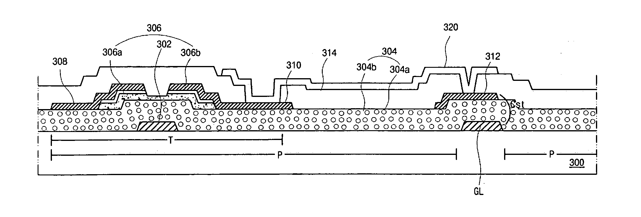
[0033]FIG. 4 is a schematic cross-sectional view showing a thin film transistor of an array substrate for a liquid crystal display device according to the present invention.

[0034]In FIG. 4, a thin film transistor (TFT) “T” includes a gate electrode 102 on a substrate 100, a gate insulating layer 104 on the gate electrode 102, a semiconductor layer 106 on the gate insulating layer 104 over the gate electrode 102, and source and drain electrodes 108 and 110 on the semiconductor layer 106. The gate insulating layer 104 may include a particle and a matrix, preferably a nano-particle 104a of an inorganic material and an organic matrix 104b of an organic material. The organic matrix 104b surrounds the nano-particle 104a and the nano-particle 104a is dispersed in the organic matrix 104b. The gate insulating layer 104 may be obtained through steps of forming a composite precursor film of a core-shell structure and curing the composite precursor film by, for example, heat or light. In additi...

second embodiment

[0044]FIG. 6 is a cross-sectional view showing an organic polymer solution used for a gate insulating layer of an array substrate for a liquid crystal display device according to the present invention.

[0045]In FIG. 6, an organic polymer melts in a solvent to constitute an organic polymer solution 202 in a vessel 200. A particle, preferably a nano-particle 204 such as zirconium oxide (ZrO2) having a dielectric constant over about 8 may be dispersed in the organic polymer solution 202. The organic polymer may include a material obtainable through a sol-gel method. For example, the organic polymer may include one of single polymer and copolymer such as siloxane polymer, polyacrylate-polyimide and polyester. In addition, the nano-particle 204 may include one of barium strontium titanate, barium zirconate titanate, lead zirconate titanate, strontium titanate, barium titanate, barium magnesium fluoride, bismuth titanate, strontium bismuth tantalate, strontium bismuth tantalate niobate and...


PUM


Abstract

An array substrate for a liquid crystal display device, including: a substrate; a gate electrode on the substrate; and a gate insulating layer including an organic matrix of an organic material and an additive that increases a dielectric constant of the gate insulating layer.

Description

[0001]This application claims the benefit of Korean Patent Application No. 2006-0031712, filed on Apr. 7, 2006, which is hereby incorporated by reference in its entirety for all purposes as if fully set forth herein.BACKGROUND OF THE INVENTION[0002]1. Field of the Invention[0003]The present invention relates to an array substrate for an LCD device including a gate insulating layer having a high dielectric constant and a method of fabricating the array substrate.[0004]2. Discussion of the Related Art[0005]Liquid crystal display (LCD) devices are widely used in televisions and as monitors for notebook and desktop computers because of their high resolution, high contrast ratio, color rendering capability and superior performance for displaying moving images. An LCD device relies on the optical anisotropy and polarizing properties of liquid crystal to produce an image. In addition, an LCD device includes a liquid crystal panel including two substrates and a liquid crystal layer between ...

Claims


Application Information

Patent Timeline
IPC IPC(8): G02F1/136
CPCG02F1/136227B82Y20/00G02F2202/36G02F1/1362G02F1/133345H01L29/42384H01L29/4908
Inventor HEO, JAE-SEOKJUN, WOONG-GICHAE, GEE-SUNG
Owner LG DISPLAY CO LTD
Why Eureka
Try Eureka