Bolometer structure, infrared detection pixel employing bolometer structure, and method of fabricating infrared detection pixel

a bolometer and infrared detection technology, applied in the manufacture of cables/conductor parts, optical radiation measurement, instruments, etc., can solve the problems of inconvenient use, deterioration of the overall netd, and material complexity, so as to improve the responsivity of the bolometer and process yield, the effect of reducing the thickness of the bolometer structur

Inactive Publication Date: 2010-06-17
ELECTRONICS & TELECOMM RES INST
View PDF2 Cites 30 Cited by
  • Summary
  • Abstract
  • Description
  • Claims
  • Application Information

AI Technical Summary

Benefits of technology

[0047]The present invention is also directed to providing a method of reducing the thickness of a bolometer structure in order to improve responsivity of a bolometer and process yield.

Problems solved by technology

To enhance the characteristics, not by improving the resistant material, but by designing the structure, is somewhat complicated.
However, the structure requires an additional process and increases the heat capacity of the bolometer structure 110, thereby deteriorating overall NETD.
Meanwhile, it is also problematic when the bias voltage Vb is not high enough in Equation 8.
This is intended to improve infrared responsivity, but may cause severe deformation.
On the other hand, when an infrared-sensitive material whose resistivity is not large is used, the structure of FIG. 2 is not useful.
However, it is impossible to separately design the structure of FIG. 2 for the two characteristics, and thus one of the characteristics cannot but deteriorate.
Also, when the electrode is designed such that the resistance matches the ROIC, infrared absorbance may deteriorate.

Method used


Image

  • Bolometer structure, infrared detection pixel employing bolometer structure, and method of fabricating infrared detection pixel
  • Bolometer structure, infrared detection pixel employing bolometer structure, and method of fabricating infrared detection pixel
  • Bolometer structure, infrared detection pixel employing bolometer structure, and method of fabricating infrared detection pixel

Examples


Embodiment Construction

[0057]Hereinafter, exemplary embodiments of the present invention will be described in detail. However, the present invention is not limited to the embodiments disclosed below but can be implemented in various forms. The following embodiments are described in order to enable those of ordinary skill in the art to embody and practice the present invention.

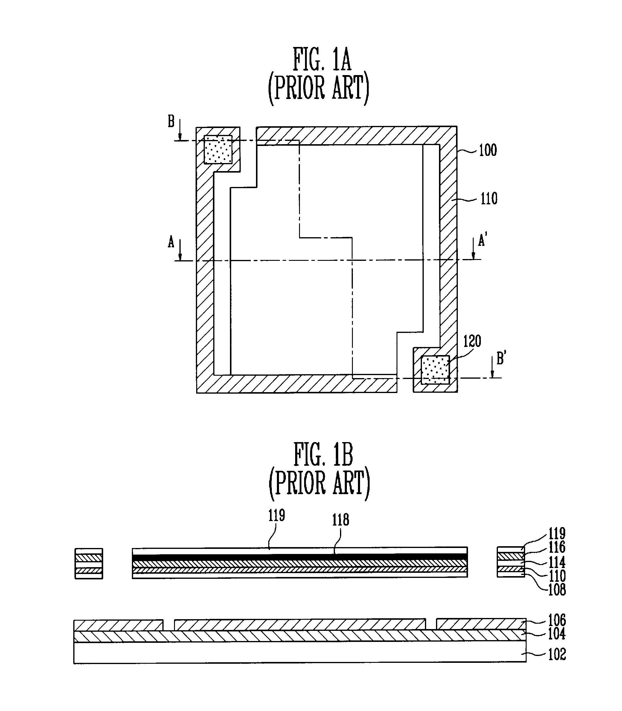
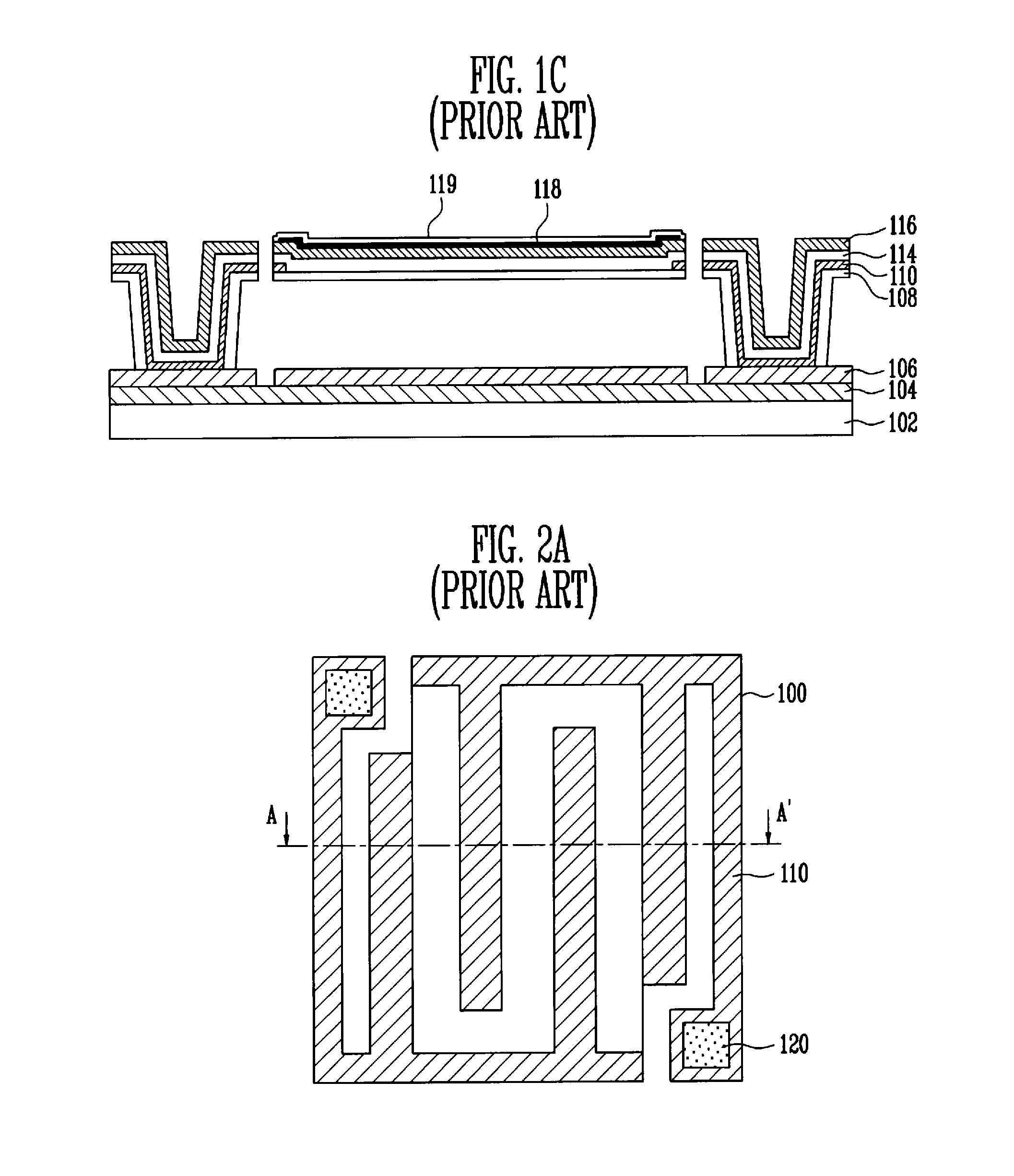
[0058]As described above, a conventional bolometer infrared sensor has a problem in that when a metal layer functioning as an absorption layer is additionally formed, an additional process is required, and overall performance deteriorates due to high heat capacity. Also, a conventional interdigitated-shape structure not requiring a metal layer functioning as an absorption layer has problems in that noise increases due to reduction in the effective volume, it is vulnerable to stress due to the asymmetry of the bolometer structure, characteristics such as thermal conductance deteriorate, and so on.

[0059]Accordingly, to solve to these p...


PUM

PropertyMeasurementUnit
thicknessaaaaaaaaaa
temperatureaaaaaaaaaa
wavelength bandaaaaaaaaaa

Abstract

Provided are a bolometer structure, an infrared detection pixel employing the bolometer structure, and a method of fabricating the infrared detection pixel.
The infrared detection pixel includes a substrate including a read-out integrated circuit (ROIC) and on which a reflection layer for reflecting infrared light is stacked, a bolometer structure formed to be spaced apart from the substrate and including a temperature-sensitive resistive layer, a first metal layer formed in a pattern on one surface of the temperature-sensitive resistive layer, a second metal layer formed in a pattern complementary to the pattern of the first metal layer on the other surface of the temperature-sensitive resistive layer in order to complementarily absorb infrared light, and an insulating layer formed between the temperature-sensitive resistive layer and the first metal layer, and a metal pad receiving a change in resistance of the temperature-sensitive resistive layer according to infrared light absorbed by the first metal layer and the second metal layer from the second metal layer, and transferring the change in resistance to the ROIC.
Thus, it is possible to improve responsivity, and implement a simple bolometer structure robust against stress. Consequently, process yield can be improved, and the volume, weight, price, etc., of application products can be reduced by reducing the volume of a bolometer structure.

Description

CROSS-REFERENCE TO RELATED APPLICATION[0001]This application claims priority to and the benefit of Korean Patent Application No. 10-2008-0127604, filed Dec. 16, 2008, the disclosure of which is incorporated herein by reference in its entirety.BACKGROUND[0002]1. Field of the Invention[0003]The present invention relates to a bolometer structure, an infrared detection pixel employing the bolometer structure and a method of fabricating the infrared detection pixel, and more particularly to a bolometer structure having a complementary absorption layer, an infrared detection pixel of a two-level structure based on micro-electro-mechanical system (MEMS) and a method of fabricating the infrared detection pixel.[0004]2. Discussion of Related Art[0005]Uncooled infrared sensors detect a change in characteristic of a material according to temperature at a normal temperature of about 300 K. An uncooled infrared sensor that detects a change in resistance is referred to as a bolometer.[0006]A bolo...

Claims


Application Information

Patent Timeline
Patent Type & Authority Applications(United States)
IPC IPC(8): G01J5/00C23F1/00
CPCG01J5/02G01J5/20G01J5/024G01J5/022H01L31/09H01L31/101
Inventor CHEON, SANG HOONRYU, HO JUNYANG, WOO SEOKCHO, SEONG MOKYU, BYOUNG GONCHOI, CHANG AUCK
Owner ELECTRONICS & TELECOMM RES INST
Why Eureka
Try Eureka