Simplified micro-bridging and roughness analysis

a micro-bridging and analysis technology, applied in the field of substrate processing, can solve the problems of not being able to solve the requirement of line width roughness (lwr), chemical processes becoming more sensitive to defects or patterning errors, and hurting process speed/leakage, so as to simplify the calculation of line edge roughness and improve process yield

Inactive Publication Date: 2012-01-31
TOKYO ELECTRON LTD
View PDF80 Cites 30 Cited by
  • Summary
  • Abstract
  • Description
  • Claims
  • Application Information

AI Technical Summary

Benefits of technology

[0009]The invention can provide apparatus and methods of processing a substrate in real-time using statistical defect procedures, models, and libraries to improve process yield. The invention provides a simple statistical algorithm that quantifies the pattern hot spot fail rate as well as the general line edge roughness for IC designs. The invention solves two problems: 1) uses a statistical method to determine the fail rate for an IC pattern site instead of exclusively using an image threshold; and 2) enables a simplified calculation of the line edge roughness that is not included in current pattern based design layout placement algorithms.
[0011]The invention creates a “hybrid” analytical algorithm that uses an experimentally determined “pooled polymer de-protection variation” (PPDV) parameter into a typical statistical distribution solution to calculate a fail rate for a specific IC design space. The invention also uses a simplified relationship to link the design space bridging fail rate to the line edge roughness using the PPDV parameter. The PPDV parameter and simplified algorithm enable an experimentally calibrated statistical optimization of IC design layouts (design rules) to produce the highest yield.

Problems solved by technology

Some resist material suppliers have solved the resolution problem and the dose problem, but have not been able to solve the line width roughness (LWR) requirement.
Chemical processes become more sensitive to defects or patterning errors when pushed to the lithography limits.
Furthermore, resist pattern hot spots show up as bridging or line edge roughness defects that can either short a functional part of the device, hurt the process speed / leakage, or hurt the long-term reliability of a chip.
Bridging and line edge roughness “hotspots” are typically difficult to simulate due to the large number of process variations like focus, dose, temperature bake uniformity, development uniformity, etc.
Accurate simulations typically require complex Monte Carlo techniques that require too much computational time to run full chip Electronic Design Automation (EDA) simulations.
However, there is no statistical description of resist response to a large number of non-ideal process effects that occur in a real manufacturing environment.

Method used


Image

  • Simplified micro-bridging and roughness analysis
  • Simplified micro-bridging and roughness analysis
  • Simplified micro-bridging and roughness analysis

Examples


Embodiment Construction

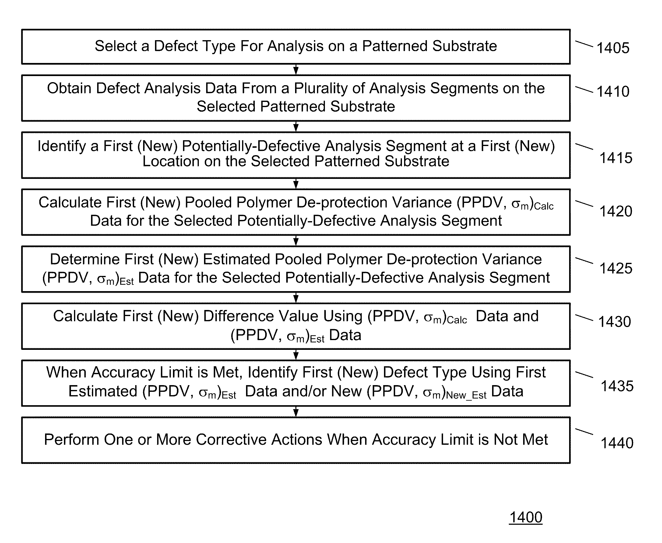
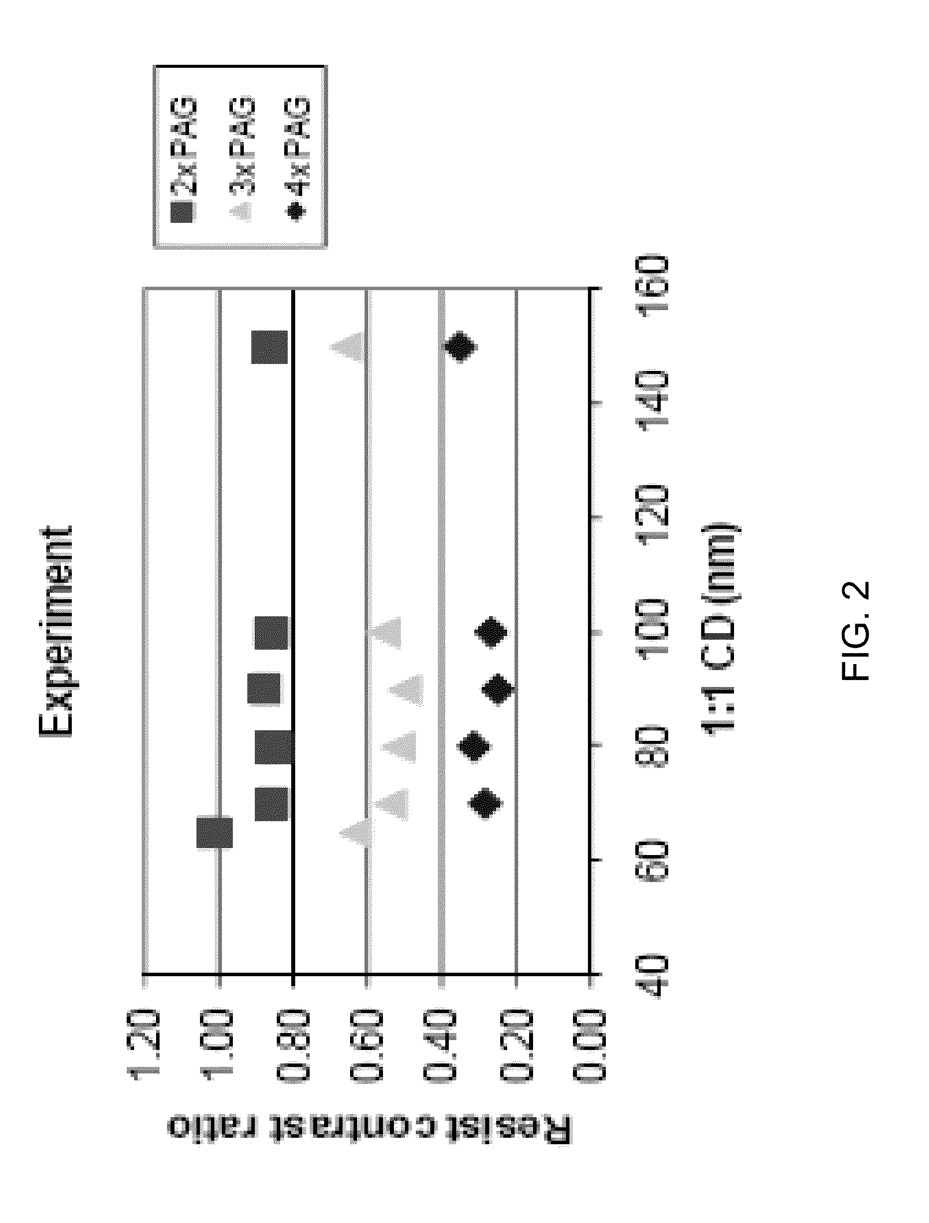
[0031]This invention provides methods and apparatus for creating calibrated resist models that capture the exposure kinetics, acid diffusion properties, de-protection kinetics, and dissolution response as a function of Photo Acid Generator (PAG) loading in 193 nm and smaller polymer systems. The invention uses calibrated resist models to quantify the resolution and sensitivity performance tradeoffs as well as the degradation of resist contrast relative to image contrast at small dimensions.

[0032]The calibrated resist simulations, which are used today, are capable of quantifying resolution and sensitivity tradeoffs, but lack the ability to model LWR. The inventor knows LWR is challenging to simulate (lattice models) and to measure due to the dependence on spectral frequency, and the inventor has developed novel techniques that use statistical data from micro-bridging experiments and historical data as means to better understand the statistical nature of LWR. Micro-bridging analysis p...


PUM


Abstract

The invention provides apparatus and methods for processing substrates using pooled statistically based variance data. The statistically based variance data can include Pooled Polymer De-protection Variance (PPDV) data that can be used to determine micro-bridging defect data, LER defect data, and LWR defect data.

Description

CROSS-REFERENCE TO RELATED APPLICATIONS[0001]This application is related to co-pending U.S. patent application Ser. No. 11 / 947,234, entitled “Enhanced Process Yield Using a Hot-Spot Library”, filed on Nov. 29, 2007. The content of this application is herein incorporated by reference in its entirety.BACKGROUND OF THE INVENTION[0002]1. Field of the Invention[0003]The present invention relates to substrate processing, and more particularly to improving the process yield using statistically dependent defect procedures and data.[0004]2. Description of the Related Art[0005]Currently used lithography processes are challenged to balance the Resolution, LWR and Sensitivity (RLS) performance tradeoffs while scaling resist thickness below 100 nm. Some resist material suppliers have solved the resolution problem and the dose problem, but have not been able to solve the line width roughness (LWR) requirement. This challenges the industry to have a deeper understanding of LWR as well as the RLS p...

Claims


Application Information

Patent Timeline
Patent Type & Authority Patents(United States)
IPC IPC(8): G06F17/50G06F17/18G06F19/00G01R27/28G01R31/00
CPCG03F7/705G03F7/70625H01L22/20H01L2924/0002H01L2924/00H01L21/67288H01L22/12
Inventor RATHSACK, BENJAMEN M
Owner TOKYO ELECTRON LTD
Why Eureka
Try Eureka