Substrate position detection apparatus, substrate position detection method, film deposition apparatus, film deposition method, and a computer readable storage medium

a position detection and substrate technology, applied in the field of substrate position, can solve the problem of inaccurate detection of substrate position, and achieve the effect of reducing detection errors in substrate position detection

Inactive Publication Date: 2010-05-20
TOKYO ELECTRON LTD
View PDF5 Cites 481 Cited by
  • Summary
  • Abstract
  • Description
  • Claims
  • Application Information

AI Technical Summary

Benefits of technology

[0014]The present invention has been made in view of the above, and provides a substrate position detection apparatus and a substrate position detection method that are capable of reducing detection errors in a substrate position detection through taking an image of a substrate; a film deposition apparatus provided with the substrate position detection apparatus; a film deposition method using the film deposition apparatus; a computer readable storage medium storing a computer program for causing the substrate position detection apparatus to perform the substrate position detection method; and a computer readable storage medium storing a computer program for causing the film deposition apparatus to perform the film deposition method.

Problems solved by technology

However, as a result of an investigation carried out by the inventors of the present invention, it has been revealed that detection errors may be caused by reflection of light when an image of a substrate is taken by a camera, and thus a position of the substrate is not accurately detected.

Method used


Image

  • Substrate position detection apparatus, substrate position detection method, film deposition apparatus, film deposition method, and a computer readable storage medium
  • Substrate position detection apparatus, substrate position detection method, film deposition apparatus, film deposition method, and a computer readable storage medium
  • Substrate position detection apparatus, substrate position detection method, film deposition apparatus, film deposition method, and a computer readable storage medium

Examples


Embodiment Construction

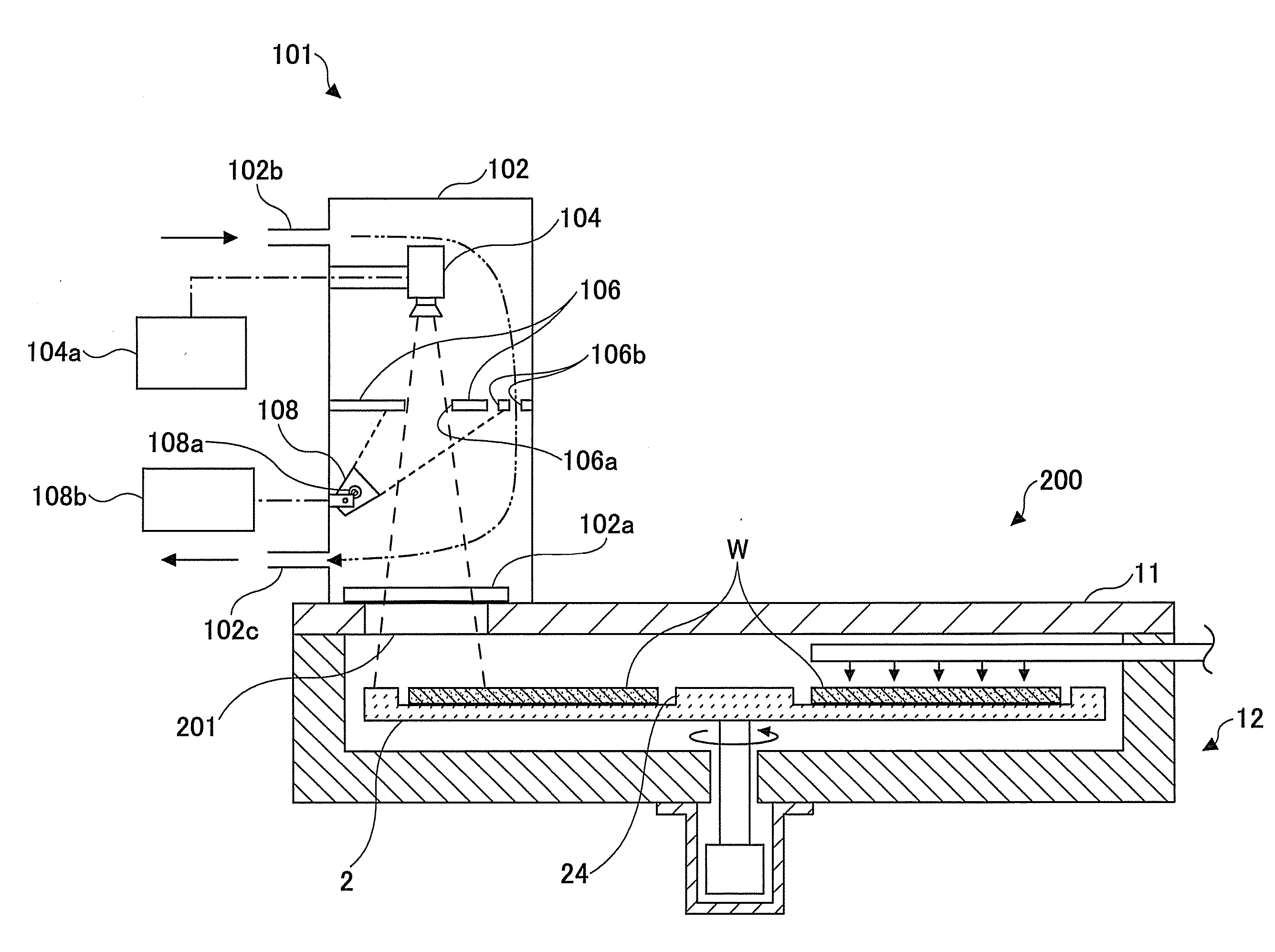
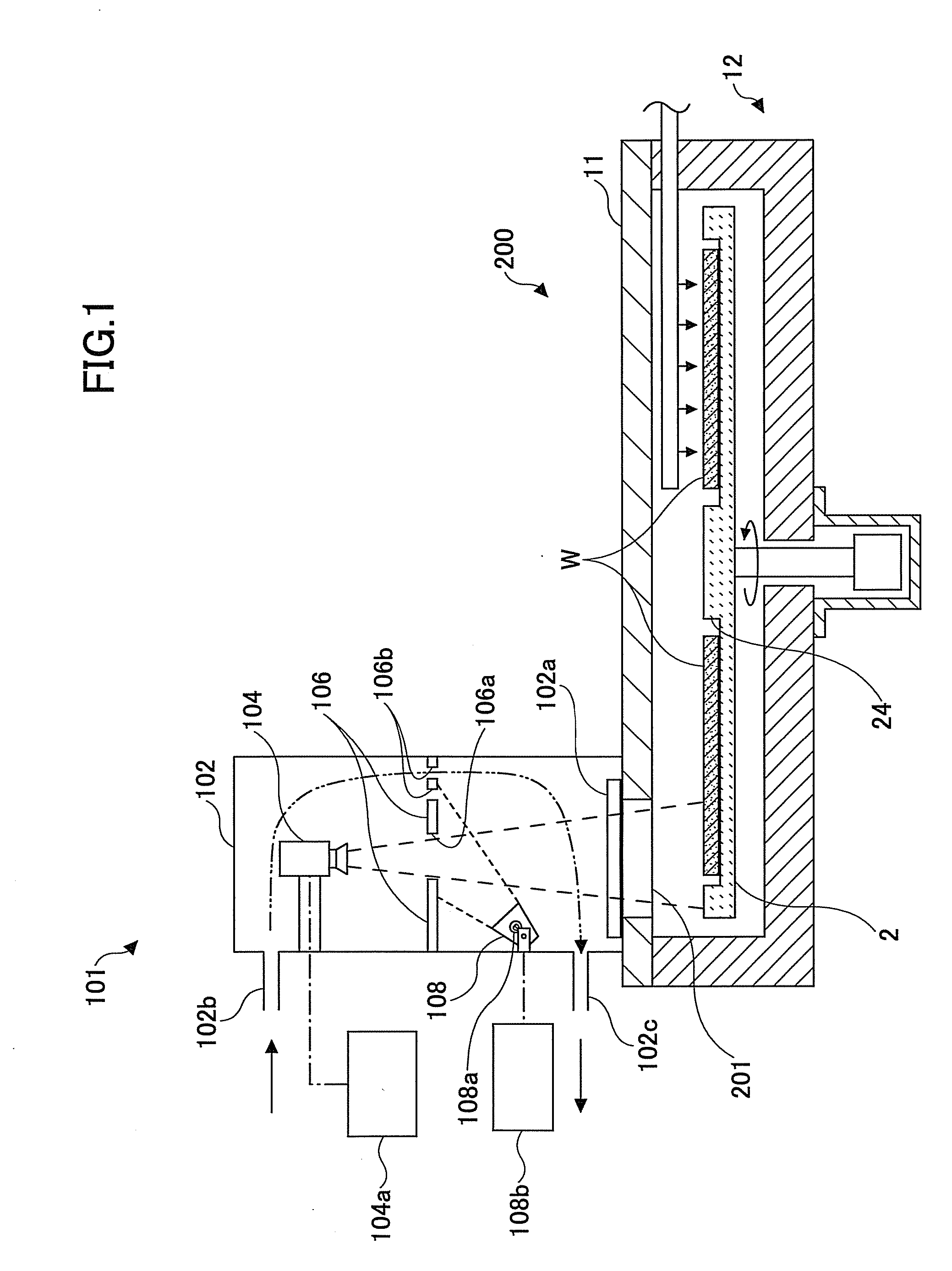
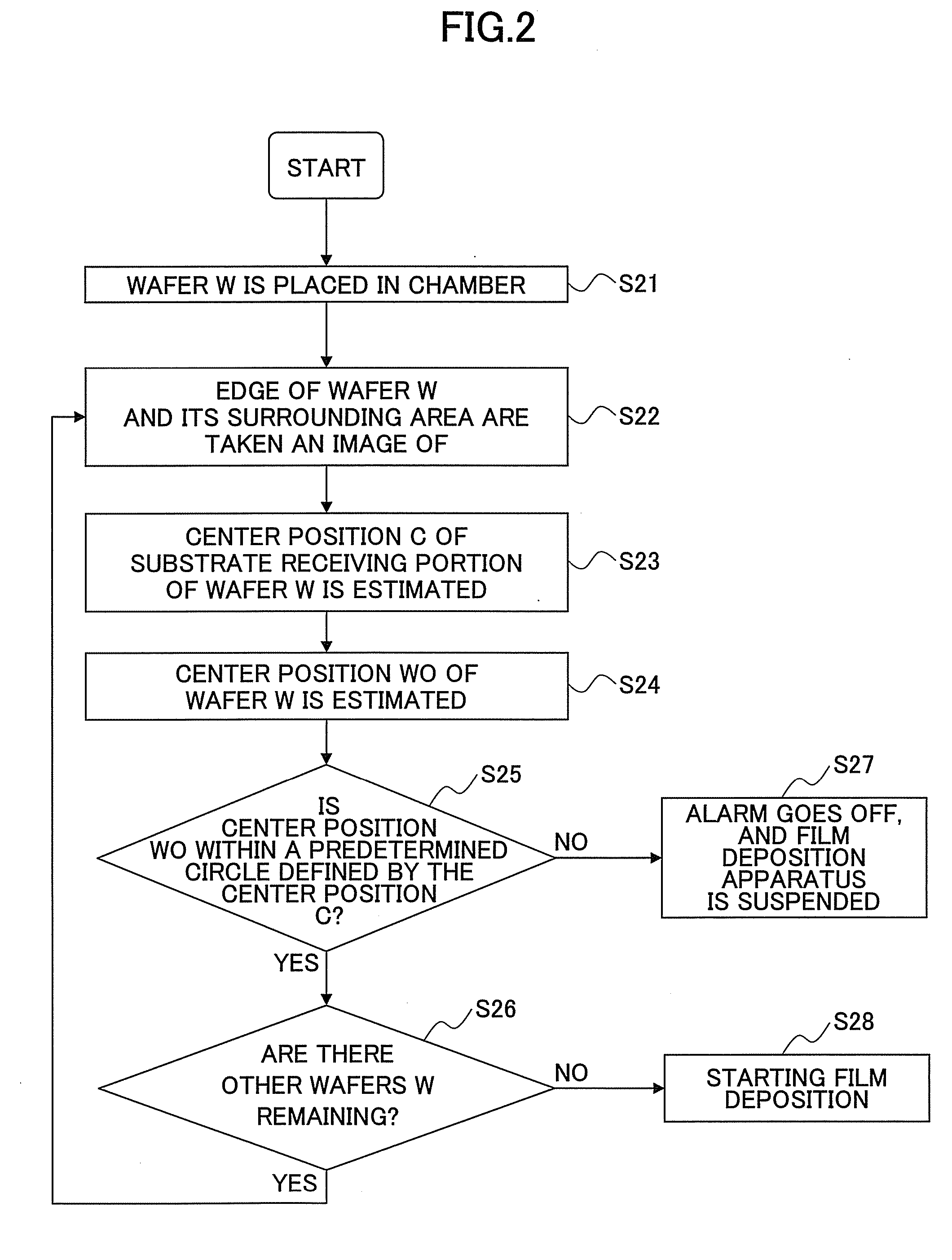
[0050]According to an embodiment of the present invention, there are provided a substrate position detection apparatus and a substrate position detection method that are capable of reducing detection errors in a substrate position detection through taking an image of a substrate; a film deposition apparatus provided with the substrate position detection apparatus; a film deposition method using the film deposition apparatus; a computer readable storage medium storing a computer program for causing the substrate position detection apparatus to perform the substrate position detection method; and a computer readable storage medium storing a computer program for causing the film deposition apparatus to perform the film deposition method.

[0051]Non-limiting, exemplary embodiments of the present invention will now be described with reference to the accompanying drawings. In the drawings, the same or corresponding reference symbols are given to the same or corresponding members or componen...


PUM

PropertyMeasurementUnit
diameteraaaaaaaaaa
diameteraaaaaaaaaa
diameteraaaaaaaaaa

Abstract

A disclosed substrate position detection apparatus includes an imaging portion configured to take an image of a substrate subject to a position detection; a panel member provided between the imaging portion and the substrate and including a first opening that ensures a field of view for the imaging portion with respect to the substrate, the panel member having a light scattering property; a first illuminating portion configured to illuminate the panel member; and a processing portion capable of determining a position of the substrate in accordance with the image taken through the first opening by the imaging portion.

Description

CROSS-REFERENCE TO RELATED APPLICATION[0001]This application claims the benefit of priority of Japanese Patent Applications No. 2008-295641 and No. 2009-130532, filed on Nov. 19, 2008 and May 29, 2009, respectively, with the Japanese Patent Office, the entire contents of which are hereby incorporated by reference.BACKGROUND OF THE INVENTION[0002]1. Field of the Invention[0003]The present invention relates to a substrate position detection apparatus and a substrate position detection method that detect a position of a substrate housed in a semiconductor device fabrication apparatus; a film deposition apparatus provided with the substrate position detection apparatus; a film deposition method performed using the film deposition apparatus; a computer readable storage medium storing a computer program for causing the substrate position detection apparatus to perform the substrate position detection method; and a computer readable storage medium storing a computer program for causing the...

Claims


Application Information

Patent Timeline
Patent Type & Authority Applications(United States)
IPC IPC(8): C23C16/00G01B11/14G01B11/00B05C11/10
CPCC23C16/4584C23C16/52H01L21/681H01L21/67259G01B11/00H01L21/68H01L21/20
Inventor AIKAWA, KATSUYOSHIHONMA, MANABU
Owner TOKYO ELECTRON LTD
Why Eureka
Try Eureka