Power Semiconductor Module with Prestressed Auxiliary Contact Spring

a technology of auxiliary contact spring and semiconductor module, which is applied in the direction of semiconductor/solid-state device details, electrical apparatus construction details, coupling device connections, etc., can solve the problems of increasing the risk of damage and excessive projection of technology, and achieve the effect of reducing the projection of the upper contact devi

Active Publication Date: 2010-05-27
SEMIKRON ELECTRONICS GMBH & CO KG
View PDF2 Cites 1 Cited by
  • Summary
  • Abstract
  • Description
  • Claims
  • Application Information

AI Technical Summary

Benefits of technology

[0012]It is therefore an object of the present invention to provide a power semiconductor module comprising pressure spring contacts, wherein the projection of the upper contact device is reduced and therefore so, too, is the risk of deformation of the contacts.

Problems solved by technology

What is disadvantageous about the prior art here is a technologically dictated excessively large projection of the auxiliary contact spring beyond the housing in the unmounted state and without arrangement of the control circuit board.
The pressure contact spring projects beyond the housing at most by its entire spring excursion, which increases the risk of damage in the form of deformation of the spring head, that is to say of the upper contact device of the auxiliary connection.

Method used


Image

  • Power Semiconductor Module with Prestressed Auxiliary Contact Spring
  • Power Semiconductor Module with Prestressed Auxiliary Contact Spring
  • Power Semiconductor Module with Prestressed Auxiliary Contact Spring

Examples


Embodiment Construction

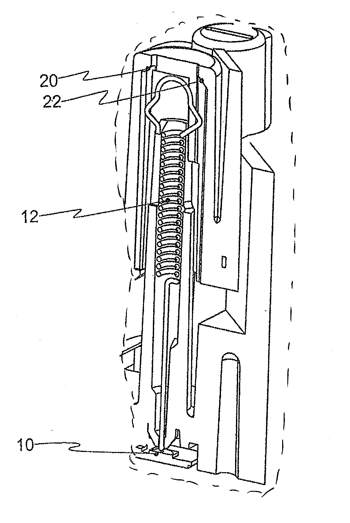
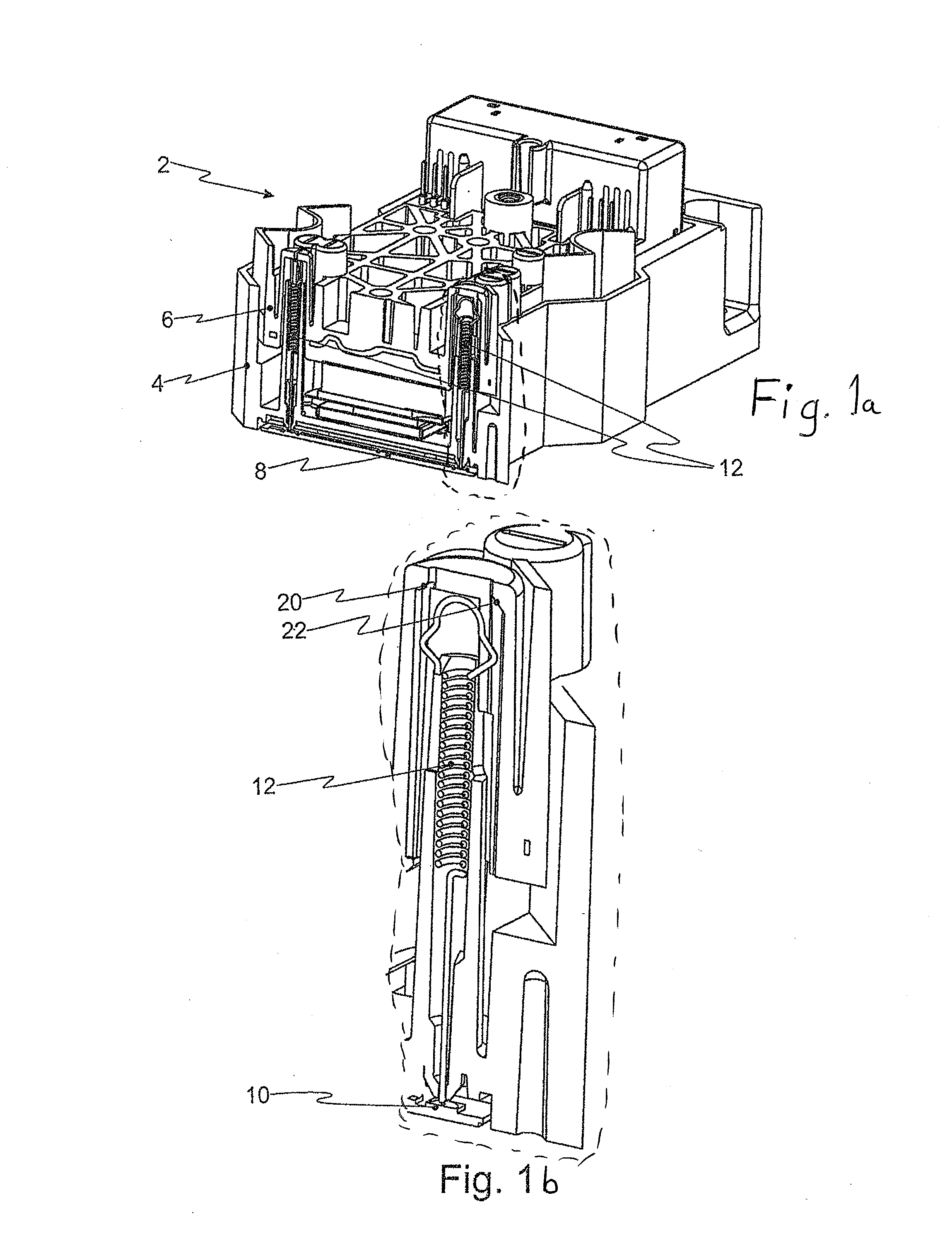
[0027]FIG. 1 is a cross-section through a power semiconductor module 2 according to the invention before the positioning of a pressure member 6 therein. In this case, the contact springs 12 (shown in detail in FIG. 1b) are arranged in movable fashion in shafts within a housing 4. Pressure member 6 is illustrated here with stop elements 20, 22. Power semiconductor module 2 likewise has a substrate 8 having contact areas 10. Contact areas 10 on substrate 8 provide electrical contact-connection of substrate 8 via contact springs 12 to control circuit boards 28 (FIG. 3) that can be mounted on power semiconductor module 2.

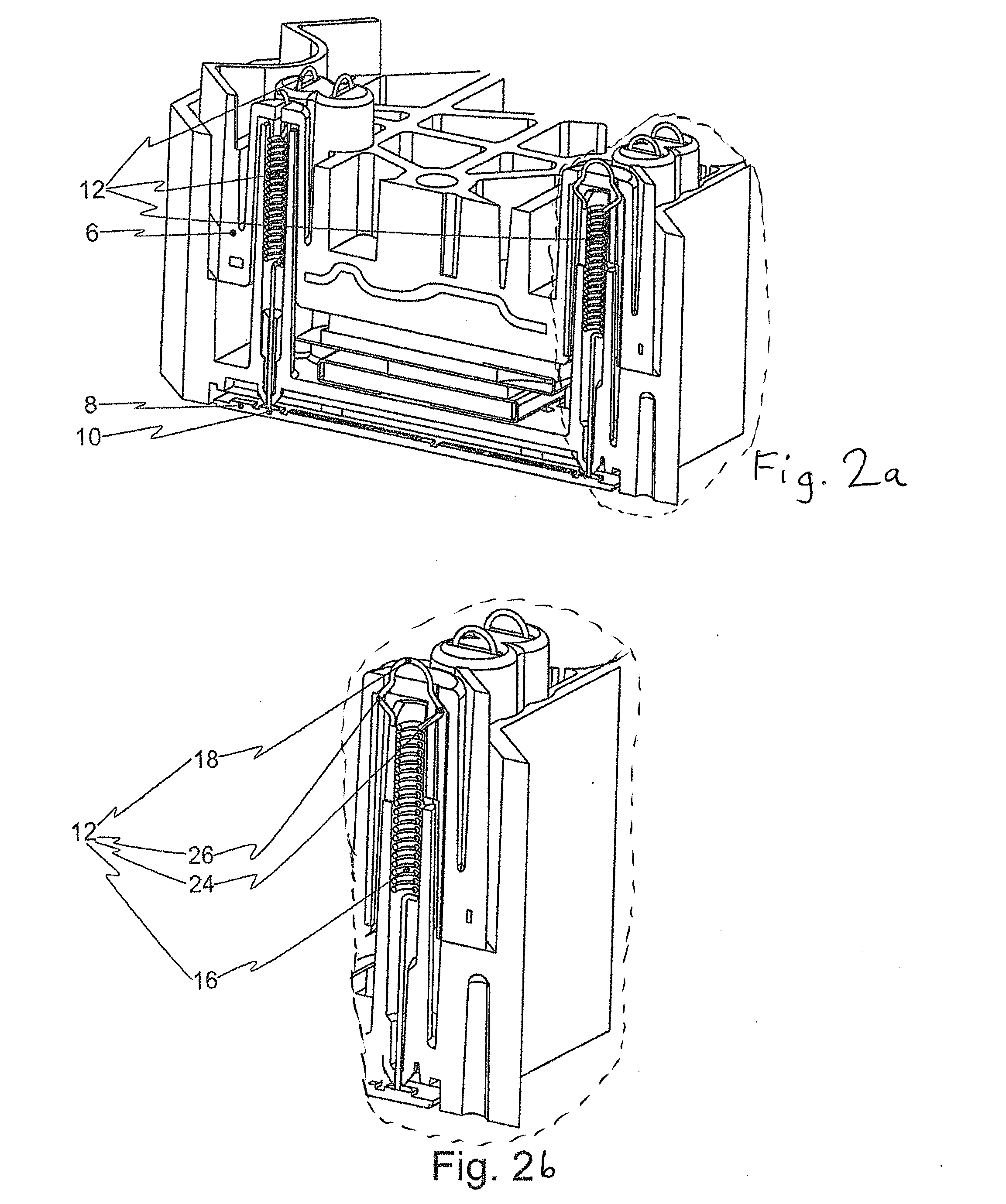
[0028]FIG. 2 is a cross-section through power semiconductor module 2 with pressure member 6 in place. As a result of the insertion of pressure member 6 pressure is applied to V-shaped deformations 24, 26 of a second contact device 18 of contact spring 12 by means of stop elements 20, 22 of pressure member 6a Deformations 24-26 thereby prestress contact spring 12. As a r...


PUM


Abstract

A power semiconductor module having a housing, a pressure member, a substrate including at least one contact surface, and at least one connection element leading towards the exterior of the housing. The connection element has a first contact device, a resilient section and a second contact device. The pressure member has two stop elements. The first contact device is electrically conductively connected to the contact surfaces of the substrate. The second contact device is arcuate in shape and has at least one deformation at the beginning and at the end of the arc, wherein, as a result of the deformations of the second contact device co-operating with the two stop elements of the pressure member, the connection element is prestressed.

Description

BACKGROUND OF THE INVENTION[0001]1. Field of the Invention[0002]The invention is directed to power semiconductor modules and, more particularly, to power semiconductor modules having a contact spring providing pressure contact to ensure electrical connection of the elements thereof.[0003]2. Description of the Related Art[0004]Know power semiconductor modules of the type described herein are described, example from German Published Patent Application DE 197 19 703 A1. Power semiconductor modules of this type comprise, according to the prior art, a housing with at least one electrically insulating substrate arranged therein, preferably for direct mounting on a cooling component. The substrate, for its part, comprises a body made up of an insulating material with a plurality of mutually insulated metallic connecting tracks situated thereon and power semiconductor components which are situated on the connecting tracks and connected to the connecting tracks in a circuit-conforming manner...

Claims


Application Information

Patent Timeline
Patent Type & Authority Applications(United States)
IPC IPC(8): H01R13/33H01R12/00
CPCH01L23/48H01L25/072H01R13/2421H05K7/1432H01L23/34H01L2924/0002H01L23/49534H01L25/16H01L2924/00H05K7/14329H01L25/00
Inventor LEDERER, MARCO
Owner SEMIKRON ELECTRONICS GMBH & CO KG
Why Eureka
Try Eureka