Semiconductor package, method of manufacturing semiconductor package, electronic component, and method of manufacturing electronic component

Inactive Publication Date: 2010-06-03
RENESAS ELECTRONICS CORP
View PDF0 Cites 13 Cited by
  • Summary
  • Abstract
  • Description
  • Claims
  • Application Information

AI Technical Summary

Benefits of technology

[0017]According to the invention, the dielectric having a relative dielectric constant higher than that of the sealing resin is disposed between the die pad having an antenna function and the semiconductor chip. Accordingly, it is possible to suppress the absorption of the RF waves in the semiconductor chip. As a result, it is possible to effectively suppress the attenuation of the electric field strength of the RF waves emitted from the package.
[0018]According to the invention, it is possible to effectively suppress the attenuation of the electric field strength of the RF waves emitted from the package.

Problems solved by technology

This is because neighboring metals such as leads, wires, and semiconductor chips interfere with each other.

Method used


Image

  • Semiconductor package, method of manufacturing semiconductor package, electronic component, and method of manufacturing electronic component
  • Semiconductor package, method of manufacturing semiconductor package, electronic component, and method of manufacturing electronic component
  • Semiconductor package, method of manufacturing semiconductor package, electronic component, and method of manufacturing electronic component

Examples


Embodiment Construction

[0030]The invention will be now described herein with reference to illustrative embodiments. Those skilled in the art will recognize that many alternative embodiments can be accomplished using the teachings of the present invention and that the invention is not limited to the embodiments illustrated for explanatory purposes.

[0031]Hereinafter, preferred embodiments of the invention will be described with reference to the accompanying drawings. In all the drawings, like elements are referenced by like reference numerals and descriptions thereof will not be repeated.

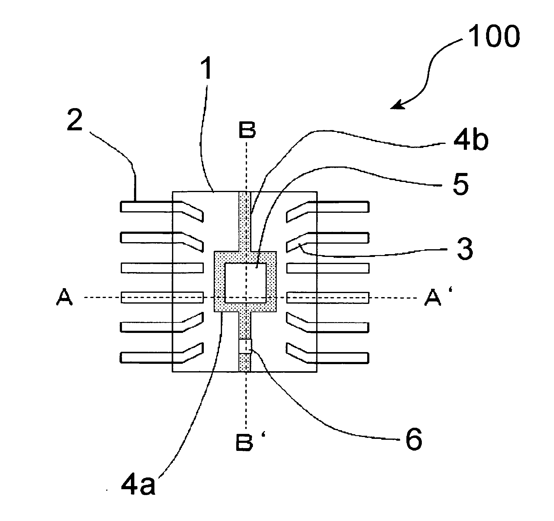
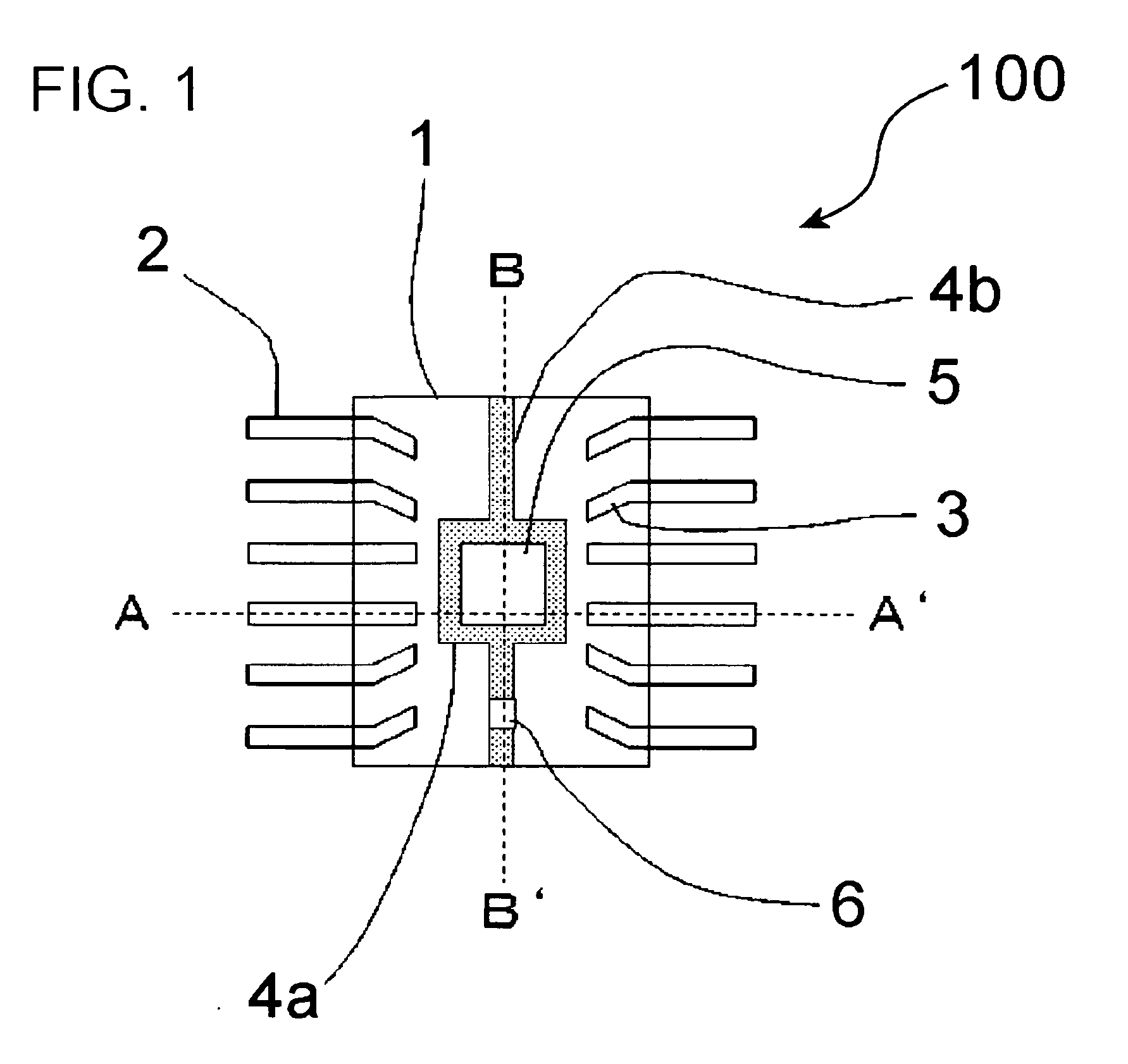
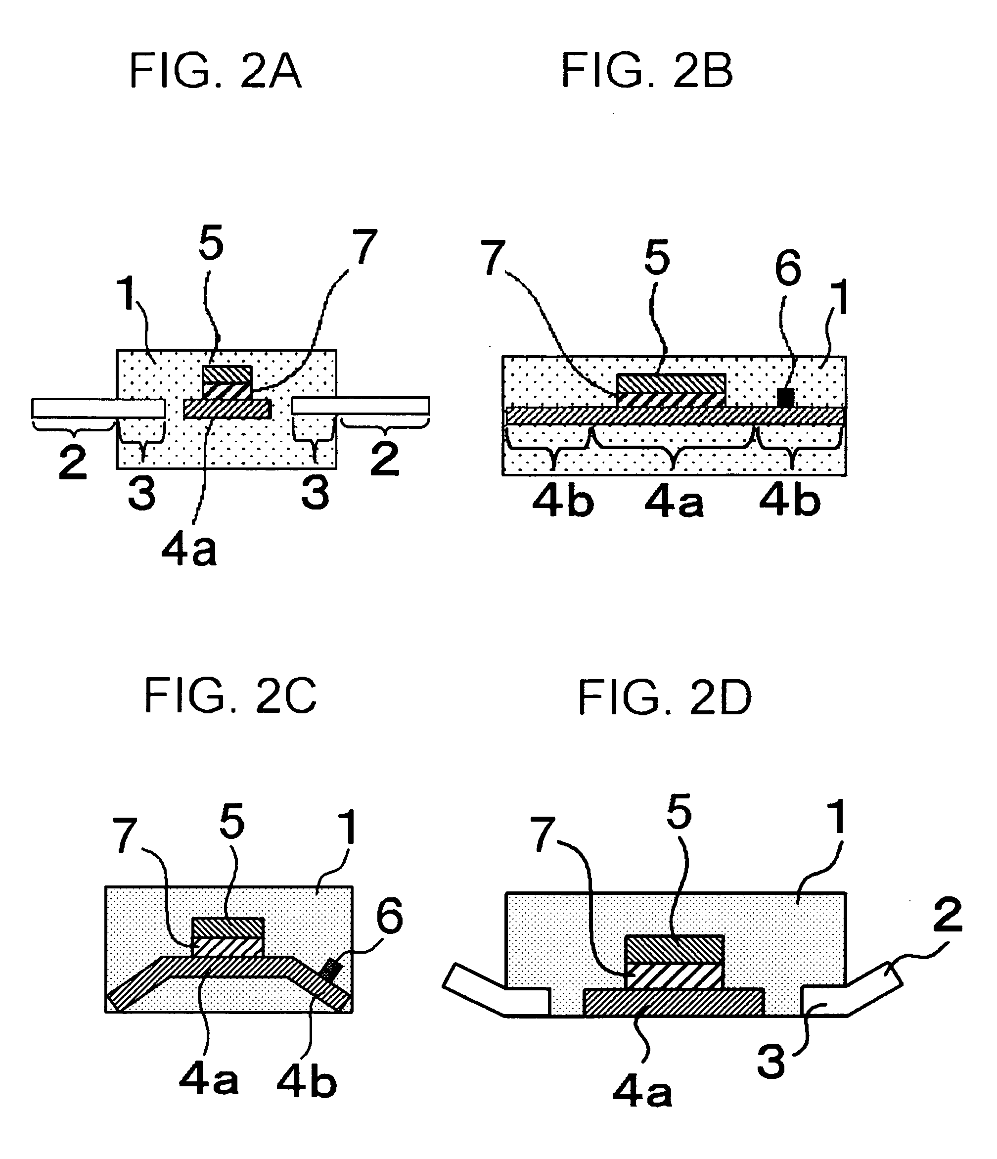
[0032]FIG. 1 is a plan (perspective) view schematically illustrating a semiconductor package 100 according to an embodiment of the invention. FIGS. 2A and 2D are sectional views taken along line A-A′ of the semiconductor package 100 shown in FIG. 1 and FIGS. 2B and 2C are sectional views taken along line B-B′ of the semiconductor package 100 shown in FIG. 1.

[0033]The semiconductor package 100 includes a semiconductor chip 5...


PUM

PropertyMeasurementUnit
Thicknessaaaaaaaaaa
Thicknessaaaaaaaaaa
Dielectric constantaaaaaaaaaa

Abstract

A semiconductor package includes a semiconductor chip, a die pad being mounted with the semiconductor chip with a dielectric interposed therebetween and serving as an antenna, and a molding resin (sealing resin) sealing the semiconductor chip and the die pad. The relative dielectric constant of the dielectric is higher than that of the sealing resin.

Description

[0001]The application is based on Japanese patent application No. 2008-306011, the content of which is incorporated hereinto by reference.BACKGROUND[0002]1. Technical Field[0003]The present invention relates to a semiconductor package, a method of manufacturing the semiconductor package, an electronic component, and a method of manufacturing the electronic component.[0004]2. Related Art[0005]For example, a semiconductor package described in Japanese Unexamined Patent Publication No. 2005-346412 has been known as a semiconductor package having a semiconductor chip and an antenna.[0006]FIG. 10 is a plan view illustrating the semiconductor package 10 described in Japanese Unexamined Patent Publication No. 2005-346412. The semiconductor package shown in FIG. 10 has a first semiconductor chip 11 such as a central processing unit (CPU) or a memory and a second semiconductor chip 12 storing an identifier, both of which are built over a lead frame 13, and the identifier is read in a non-con...

Claims


Application Information

Patent Timeline
IPC IPC(8): G06K19/07H01L23/552H01Q17/00H01L21/56
CPCG06K19/07771H01L23/3107H01L2924/12041H01L2924/00014Y10T29/49018H01L2924/181H01L2924/01006H01L24/48H01L24/32H01L2924/01033H01Q1/2283H01L2924/1433H01L2924/14H01L2924/09701H01L2924/01082H01L2924/01074H01L2924/01047H01L2924/01005H01L2224/92247H01L2224/73265H01L23/495H01L23/49513H01L23/49541H01L23/49575H01L23/552H01L23/66H01L2223/6677H01L2224/32245H01L2224/48091H01L2224/48247H01L2924/00H01L2224/45099H01L2224/45015H01L2924/207H01L2924/00012
Inventor SHINGAI, TADAYUKI
Owner RENESAS ELECTRONICS CORP
Why Eureka
Try Eureka