Method for producing light-emitting device

Active Publication Date: 2019-02-28
TOYODA GOSEI CO LTD
View PDF7 Cites 0 Cited by
  • Summary
  • Abstract
  • Description
  • Claims
  • Application Information

AI Technical Summary

Benefits of technology

The patent aims to enhance the reflectance of a mounting substrate. This can be summarized as improving the ability of the substrate to reflect light.

Problems solved by technology

However, there are irregularities on the surface of the AlN substrate.
Even if the DBR layer or the reflective metal layer is formed, reflectance cannot be sufficiently increased.
Therefore, processing is difficult and costs much.
There was a problem that the crystal grains on the surface are removed by grinding the surface for flattening, resulting in the worsening of surface flatness.
When surface flattening is insufficient, reflectance is not sufficiently improved.

Method used


Image

  • Method for producing light-emitting device
  • Method for producing light-emitting device
  • Method for producing light-emitting device

Examples


embodiment 1

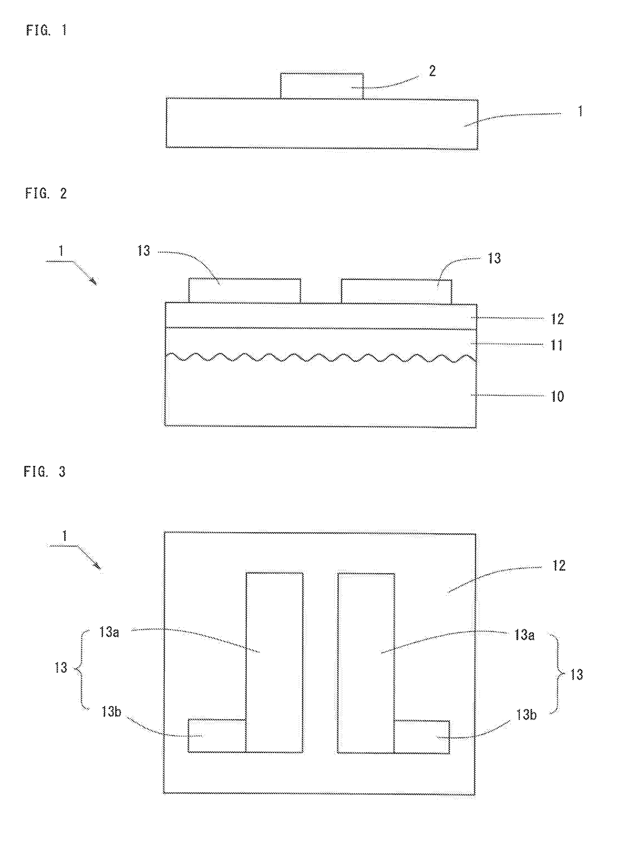
[0021]FIG. 1 shows the structure of a light-emitting device according to Embodiment 1. As shown in FIG. 1, the light-emitting device according to Embodiment 1 has a mounting substrate 1 and a light-emitting device 2, and the light-emitting diode 2 is mounted on the mounting substrate 1. The light-emitting diode 2 may have any conventionally known structure, and may be covered with a resin layer mixed with phosphor. For example, a white light-emitting diode may be achieved by having a structure in which a blue light-emitting diode 2 is covered with a resin layer mixed with yellow phosphor.

[0022]Next will be described the structure of the mounting substrate 1 in detail. The mounting substrate 1 has a substrate 10, a metal layer 11 formed on the substrate 10, a dielectric layer 12 formed on the metal layer 11, and an electrode layer 13 formed on the dielectric layer 12 as shown in FIG. 2.

[0023]The substrate 10 is formed of AlN, and has irregularities on the surface thereof, and the sur...

embodiment 2

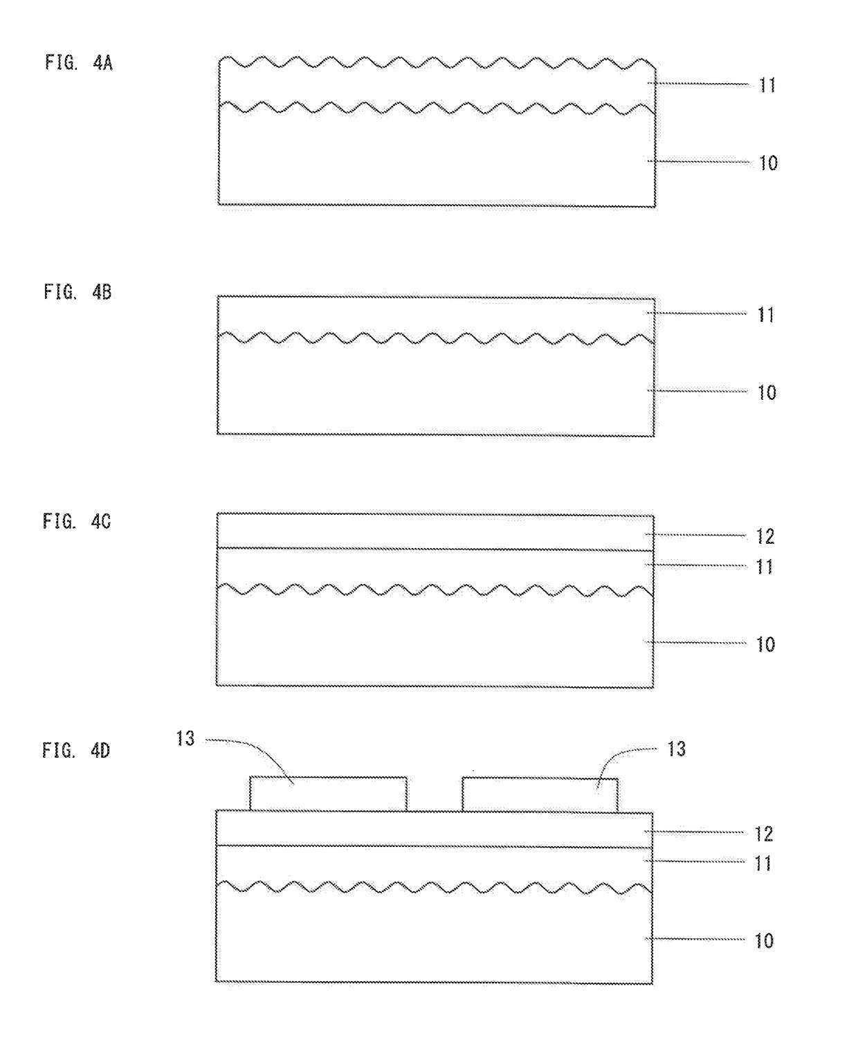
[0050]In a method for producing a light-emitting device according to Embodiment 2, the processes for producing a mounting substrate 1 in the method for producing a light-emitting device according to Embodiment 1 are changed as follows. The description of the processes until FIG. 4B are omitted because they are the same between Embodiments 1 and 2.

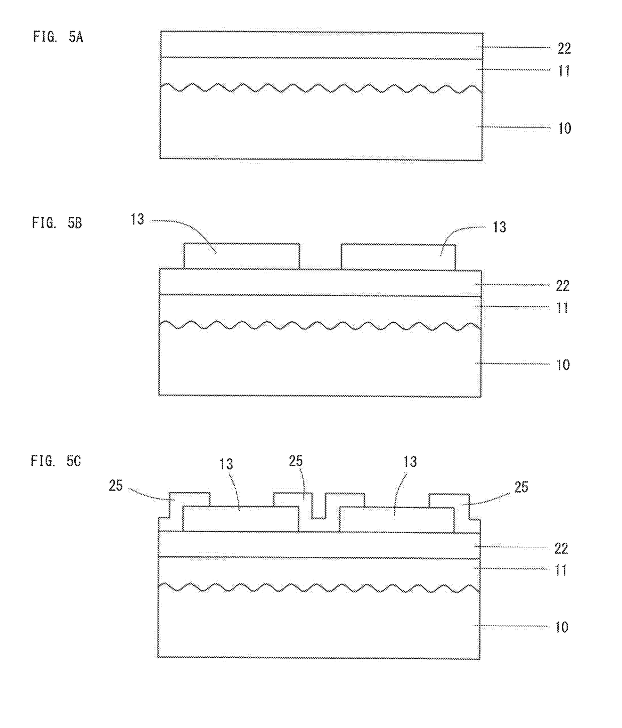
[0051]In Embodiment 2, after the surface of the metal layer 11 is ground, a dielectric layer 22 made of SiO2 having a thickness of 300 nm is formed through CVD on the metal layer 11 (refer to FIG. 5A). The dielectric layer 22 may be a dielectric multilayer film as in Embodiment 1. When a metal with low reflectance is used as the metal layer 11, a reflective metal layer 15 made of a metal with high reflectance is preferably formed between the metal layer 11 and the dielectric layer 12 as in Embodiment 1.

[0052]Subsequently, an electrode layer 13 is formed in the same pattern as in Embodiment 1 is formed by vapor deposition or lift-off on the ...


PUM


Abstract

A metal layer is formed by vapor deposition or sputtering on an AlN substrate. Since there are irregularities on the surface of the substrate, irregularities are also formed on the surface of the metal layer. Subsequently, irregularities on the surface of the metal layer are removed and flattened in a mirror state by grinding the surface of the metal layer. Then, a dielectric layer is formed on the metal layer by alternately forming a SiO2 film and a TiO2 film through CVD. Next, an electrode layer is formed in a predetermined pattern by vapor deposition and lift-off on the dielectric layer. Since the surface of the metal layer is flattened in a mirror state, reflectance is high on that surface. As a result, the emission efficiency of the light-emitting device can be improved.

Description

BACKGROUND OF THE INVENTIONField of the Invention[0001]The present invention relates to a method for producing a light-emitting device having a light-emitting diode mounted on a mounting substrate, specifically the method having a feature in a method for producing a mounting substrate.Background Art[0002]In a LED package for flowing large current such as a vehicle headlamp, an AlN substrate having insulation properties and high heat transfer characteristics is often used. To increase light extraction efficiency, light emitted from the LED to the AlN substrate is preferably reflected. Therefore, a DBR (Distributed Bragg Reflector) layer or a metal layer made of a high reflective metal such as Ag may be formed on the AlN substrate. However, there are irregularities on the surface of the AlN substrate. Even if the DBR layer or the reflective metal layer is formed, reflectance cannot be sufficiently increased.[0003]Japanese Patent Application Laid-Open (kokai) No. 2007-266647 discloses ...

Claims


Application Information

Patent Timeline
IPC IPC(8): H01L33/00H01L33/10H01L33/38
CPCH01L33/0075H01L33/10H01L33/38H01L33/486H01L33/60
Inventor TOTANI, SHINGO
Owner TOYODA GOSEI CO LTD
Why Eureka
Try Eureka