Liquid crystal display and manufacturing method thereof

a technology of liquid crystal display and manufacturing method, which is applied in the field of liquid crystal display, can solve the problems of conductive sealant deterioration, gap deterioration between the upper substrate, and height difference between the conductive sealants disposed inside the contact, so as to prevent the gap deterioration, reduce the thickness difference of conductive sealants in the contact, and minimize contact deterioration

Active Publication Date: 2010-06-03
SAMSUNG DISPLAY CO LTD
View PDF5 Cites 30 Cited by
  • Summary
  • Abstract
  • Description
  • Claims
  • Application Information

AI Technical Summary

Benefits of technology

[0007]According to exemplary embodiments of the present invention, a height difference of conductive sealants in an LCD is reduced, thereby preventing the gap deterioration between the upper and lower substrates and minimizing the contact deterioration between the common pad of the lower substrate and the common electrode of the upper substrate.

Problems solved by technology

However, when the conductive sealants overlap the contact hole, a height difference occurs between the conductive sealants disposed inside of the contact hole and the conductive sealants disposed outside of the contact hole.
The height difference according to positions of the conductive sealants generates a contact deterioration between the common pad and the common electrode, and a gap deterioration between the upper substrate and the lower substrate.

Method used


Image

  • Liquid crystal display and manufacturing method thereof
  • Liquid crystal display and manufacturing method thereof
  • Liquid crystal display and manufacturing method thereof

Examples


Embodiment Construction

[0034]The present invention will be described more fully hereinafter with reference to the accompanying drawings, in which exemplary embodiments of the invention are shown. This invention may, however, be embodied in many different forms and should not be construed as limited to the exemplary embodiments set forth herein.

[0035]It will be understood that when an element such as a layer, film, region, or substrate is referred to as being “on” another element, it can be directly on the other element or intervening elements may also be present.

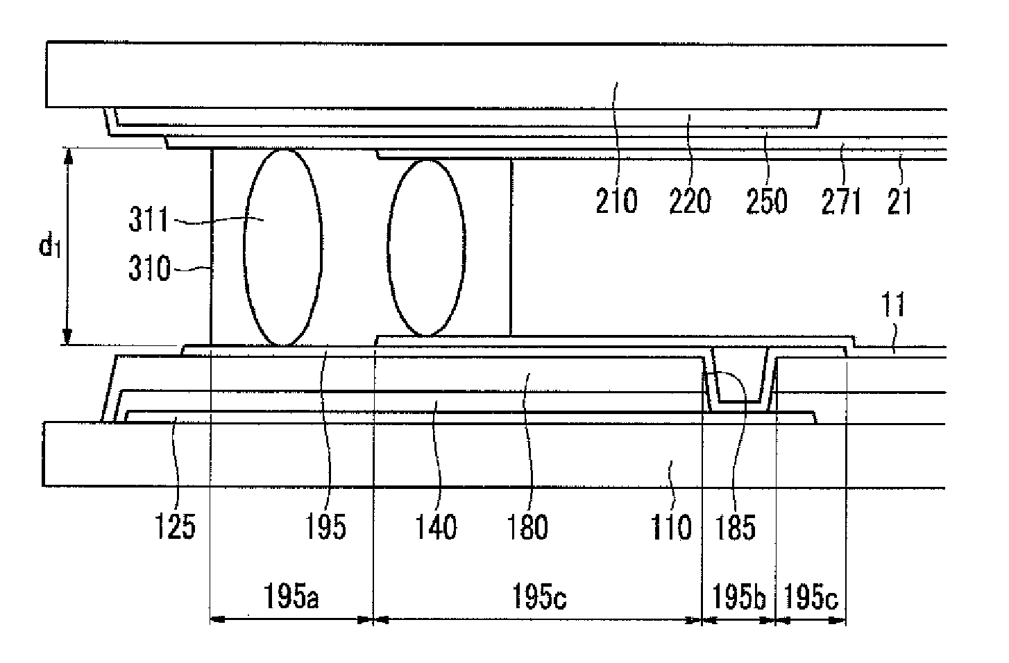
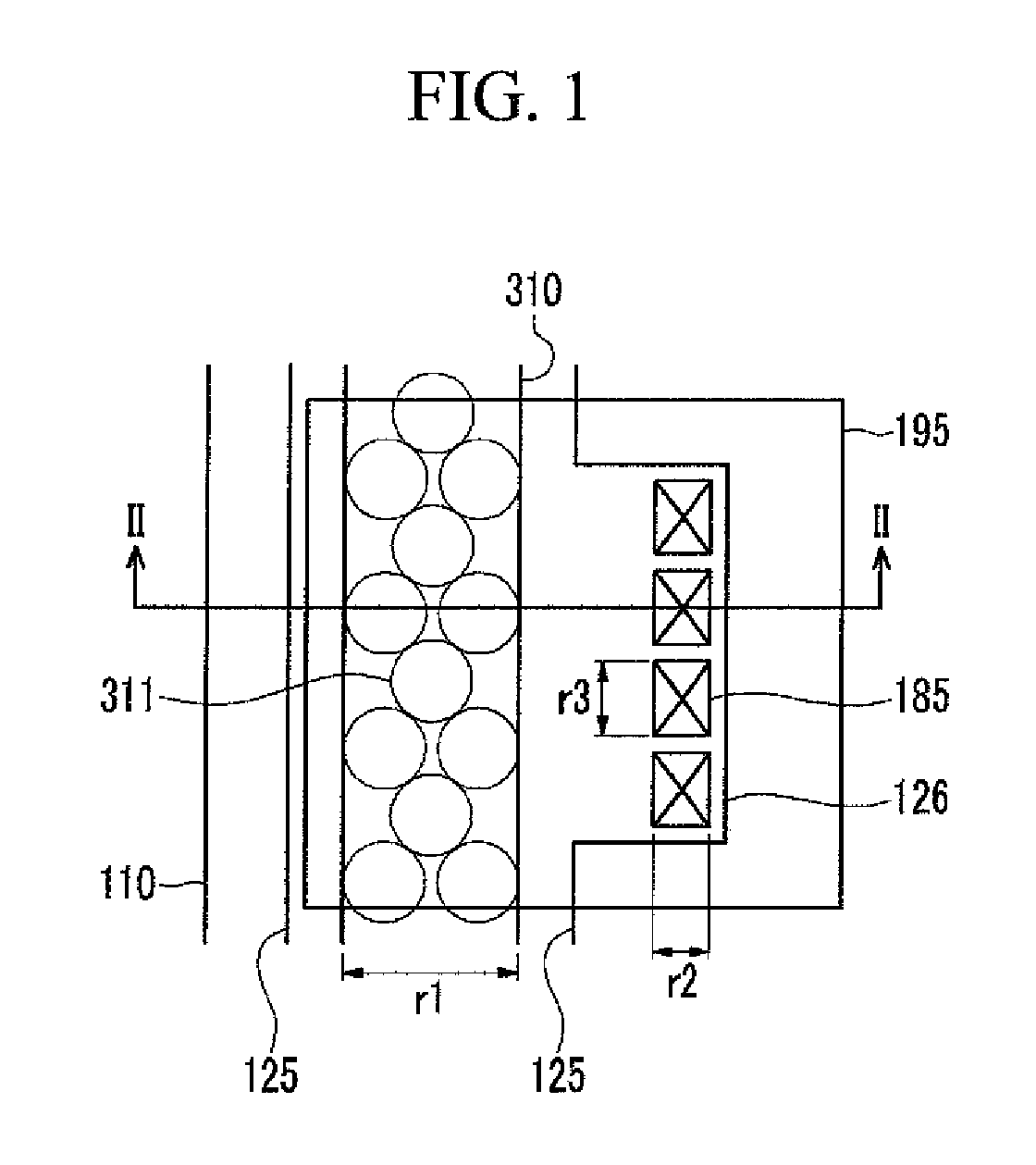
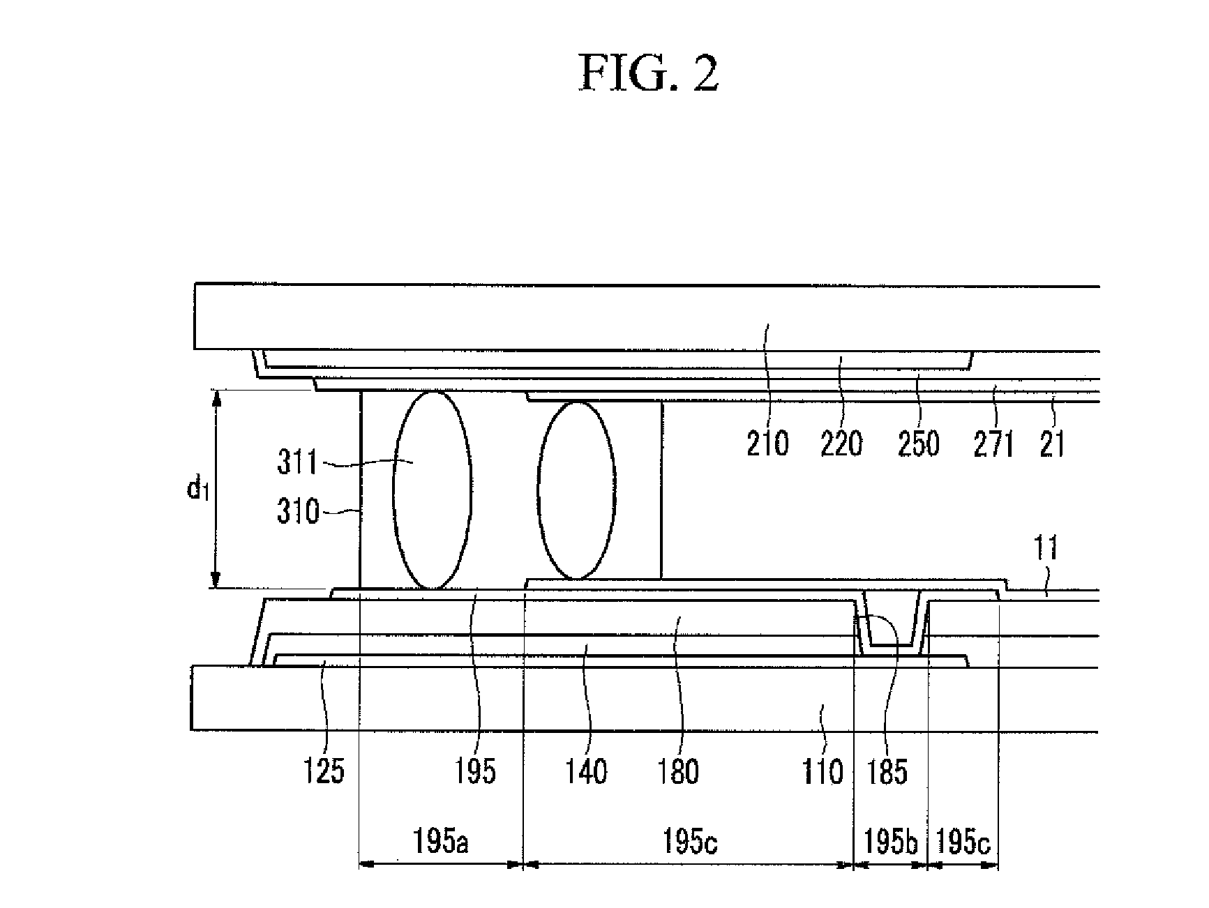
[0036]FIG. 1 is a layout view of a peripheral area of a liquid crystal display (LCD) according to an exemplary embodiment of the present invention. FIG. 2 is a cross-sectional view taken along the line II-II of FIG. 1 according to an exemplary embodiment of the present invention.

[0037]A liquid crystal display (LCD) according to an exemplary embodiment of the present invention includes a display area displaying images, and a peripheral area surroun...


PUM

PropertyMeasurementUnit
longitudinal lengthaaaaaaaaaa
diameteraaaaaaaaaa
diameteraaaaaaaaaa

Abstract

A liquid crystal display (LCD) includes a first substrate including a display area displaying images and a peripheral area surrounding the display area, a common pad formed in the peripheral area of the first substrate, an insulating layer formed on the common pad and having a common contact hole exposing the common pad, an assistance common pad formed on the insulating layer of the peripheral area and contacting the common pad through the common contact hole, a second substrate corresponding to the first substrate, and a common electrode formed on the second substrate, and a conductive sealant disposed between the assistance common pad and the common electrode of the peripheral area, the conductive sealant electrically connecting the assistance common pad and the common electrode, wherein the common contact hole is disposed between the conductive sealant and the display area.

Description

CROSS-REFERENCE TO RELATED APPLICATION[0001]This application claims priority to Korean Patent Application No. 10-20080121292 filed on Dec. 2, 2008, the entire contents of which are incorporated herein by reference.BACKGROUND OF THE INVENTION[0002](a) Technical Field[0003]The present disclosure relates to a liquid crystal display (LCD) and a manufacturing method thereof, and more particularly to an LCD having a conductive sealant and a manufacturing method thereof.[0004](b) Discussion of the Related Art[0005]Liquid crystal displays (LCDs) are used in flat panel displays. An LCD includes a pair of panels provided with field-generating electrodes and a liquid crystal (LC) layer interposed between the two panels. The LCD displays images by applying voltages to the field-generating electrodes to generate an electric field in the LC layer that determines the orientations of LC molecules therein to adjust the polarization of incident light.[0006]The LCD includes a display area displaying i...

Claims


Application Information

Patent Timeline
Patent Type & Authority Applications(United States)
IPC IPC(8): G02F1/1339
CPCG02F1/1341G02F1/136227G02F1/13458G02F1/1339G02F1/1345
Inventor LEE, SANG-KUEONHONG, KWEON-SAMPARK, HYUNKIM, SEUNG-HWAN
Owner SAMSUNG DISPLAY CO LTD
Why Eureka
Try Eureka