Method for low power accessing a phase change memory device

Active Publication Date: 2010-07-01
MICRON TECH INC
View PDF3 Cites 3 Cited by
  • Summary
  • Abstract
  • Description
  • Claims
  • Application Information

AI Technical Summary

Benefits of technology

[0021]The object of the invention is thus to solve the problem outlined above, and in particular to allow parallel writing of more than one datum each time.

Problems solved by technology

In such a situation, parallel writing of D0, D1 on a wordline may require a high write current and cause a high voltage drop on the selected wordline.
Therefore, parallel writing of two data may cause an inacceptable dissipation in the memory array, preventing in practice the parallel writing of more than one datum.

Method used


Image

  • Method for low power accessing a phase change memory device
  • Method for low power accessing a phase change memory device
  • Method for low power accessing a phase change memory device

Examples


Embodiment Construction

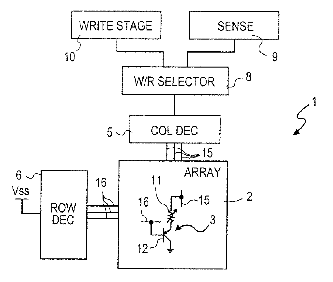
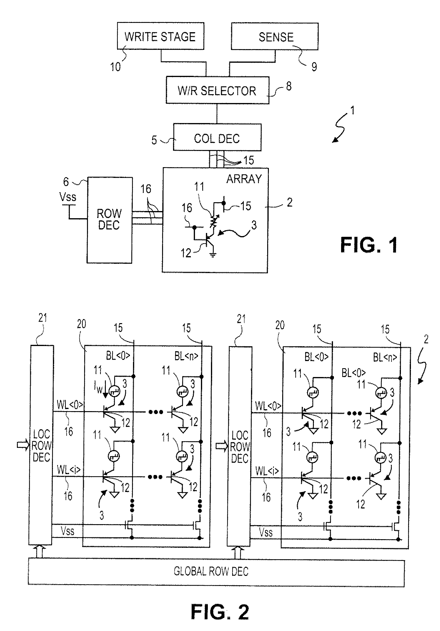
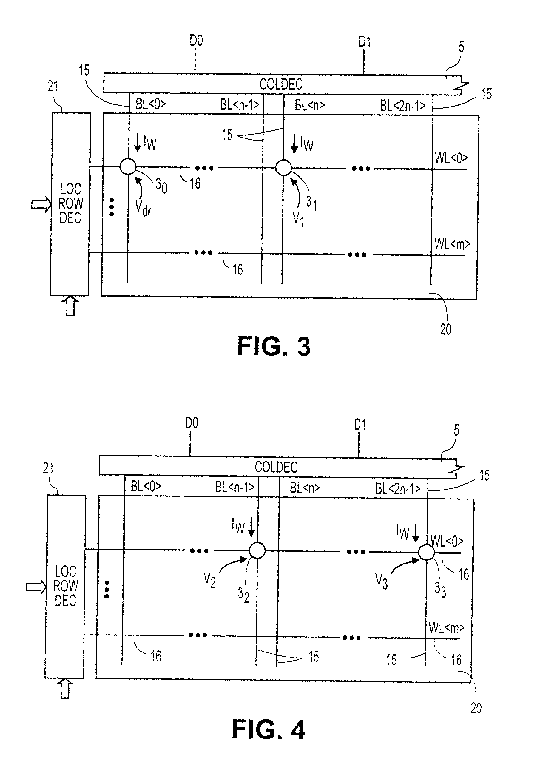
[0032]According to FIG. 5 and 6, the present method of parallel accessing memory cells 3 in an array 2 is based on varying the relative position of the addressed cells for each datum so as to minimize the worst-case current flowing in the selected wordline.

[0033]In particular, instead of simultaneously accessing cells in the same relative position within the respective datum, the order is reversed, so that, when the nearest cell 30 of D0 (connected to bitline BL0>) is accessed, the farthest cell 33 of D1 (connected to bitline BL2n+1>) is accessed, as shown in FIG. 5.

[0034]Furthermore, when the farthest cell 32 of D0 (connected to bitline BL) is accessed, the nearest cell 31 of D1 is accessed, as shown in FIG. 6.

[0035]In such a case, the voltage on the control terminal of cell 30 connected to bitline BL0> is again equal to driver voltage Vdr. The voltage V4 on the control terminal of cell 33 connected to bitline BL2n−1> is here due only to the sum of driver voltage Vdr and the voltag...


PUM


Abstract

A method for accessing a phase change memory device, wherein a first sub-plurality of bitlines is grouped in a first group and a second sub-plurality of bitlines is grouped in a second group. At least a bitline in the first and second groups are selected; currents are supplied to the selected bitlines; and a selected wordline is biased. The bitlines are selected by selecting a first bitline in the first group and, while the first bitline is selected, selecting a second bitline in the second group which is arranged on the selected wordline symmetrically to the first bitline in the first group.

Description

BACKGROUND OF THE INVENTION[0001]1) Field of the Invention[0002]Embodiments of the present invention relate to a method for low power accessing a phase change memory device.[0003]2) Description of Related Art[0004]As is known, phase change memories are formed by memory cells connected at the intersections of bitlines and wordlines and comprising each a memory element and a selection element. A memory element comprises a phase change region made of a phase change material, i.e., a material that may be electrically switched between a generally amorphous and a generally crystalline state across the entire spectrum between completely amorphous and completely crystalline states.[0005]Typical materials suitable for the phase change region of the memory elements include various chalcogenide elements. The state of the phase change material is non-volatile, absent application of excess temperatures, such as those in excess of 150° C., for extended times. Therefore, when a memory element is s...

Claims


Application Information

Patent Timeline
IPC IPC(8): G11C11/00G11C8/00
CPCG11C8/10G11C11/5678G11C13/0004G11C13/0069G11C2013/0078G11C2213/79G11C13/02G11C16/24G11C16/08
Inventor RESTA, CLAUDIOBEDESCHUI, FERDINANDO
Owner MICRON TECH INC
Why Eureka
Try Eureka