
Semiconductor light-emitting device as well as light source device and lighting system including the same

a technology of semiconductor devices and light sources, applied in semiconductor devices, solid-state devices, electric lighting sources, etc., to achieve the effect of low cos

Inactive Publication Date: 2010-07-15
PANASONIC CORP
View PDF21 Cites 49 Cited by
  • Summary
  • Abstract
  • Description
  • Claims
  • Application Information

AI Technical Summary

Benefits of technology

[0124]According to the present invention, small-sized, compact, high-power, highly reliable semiconductor light-emitting devices (for example, white LEDs) and light source devices that can be produced at low cost and can allow a circuit design to be made with precautions for lighting failure can be provided by using orthodox practical techniques.
[0125]Furthermore, a lighting system can be provided that can be restored instantly without replacing the semiconductor light-emitting device and light source even if the wiring joint portion is disconnected and thereby lighting failure is caused.

Problems solved by technology

However, it is not intended to mount a plurality of chips with high density, and the conductor pattern has a shape similar to a rectangular parallelepiped shape having line symmetry but no rotational symmetry.

Method used


Image

  • Semiconductor light-emitting device as well as light source device and lighting system including the same
  • Semiconductor light-emitting device as well as light source device and lighting system including the same
  • Semiconductor light-emitting device as well as light source device and lighting system including the same

Examples


embodiment 1

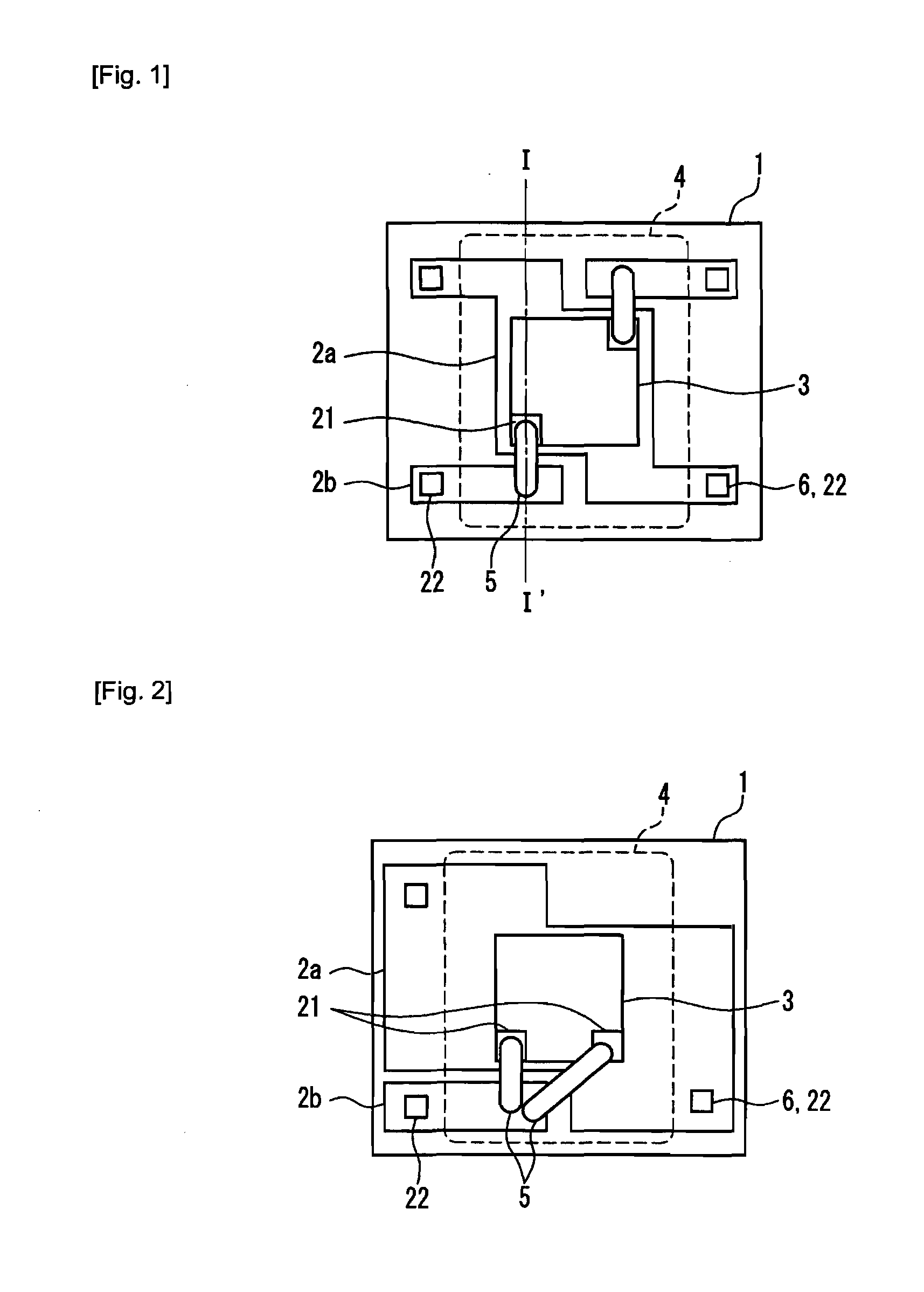
[0355]Hereinafter, Embodiment 1 of the semiconductor light-emitting device of the present invention is described with reference to drawings.

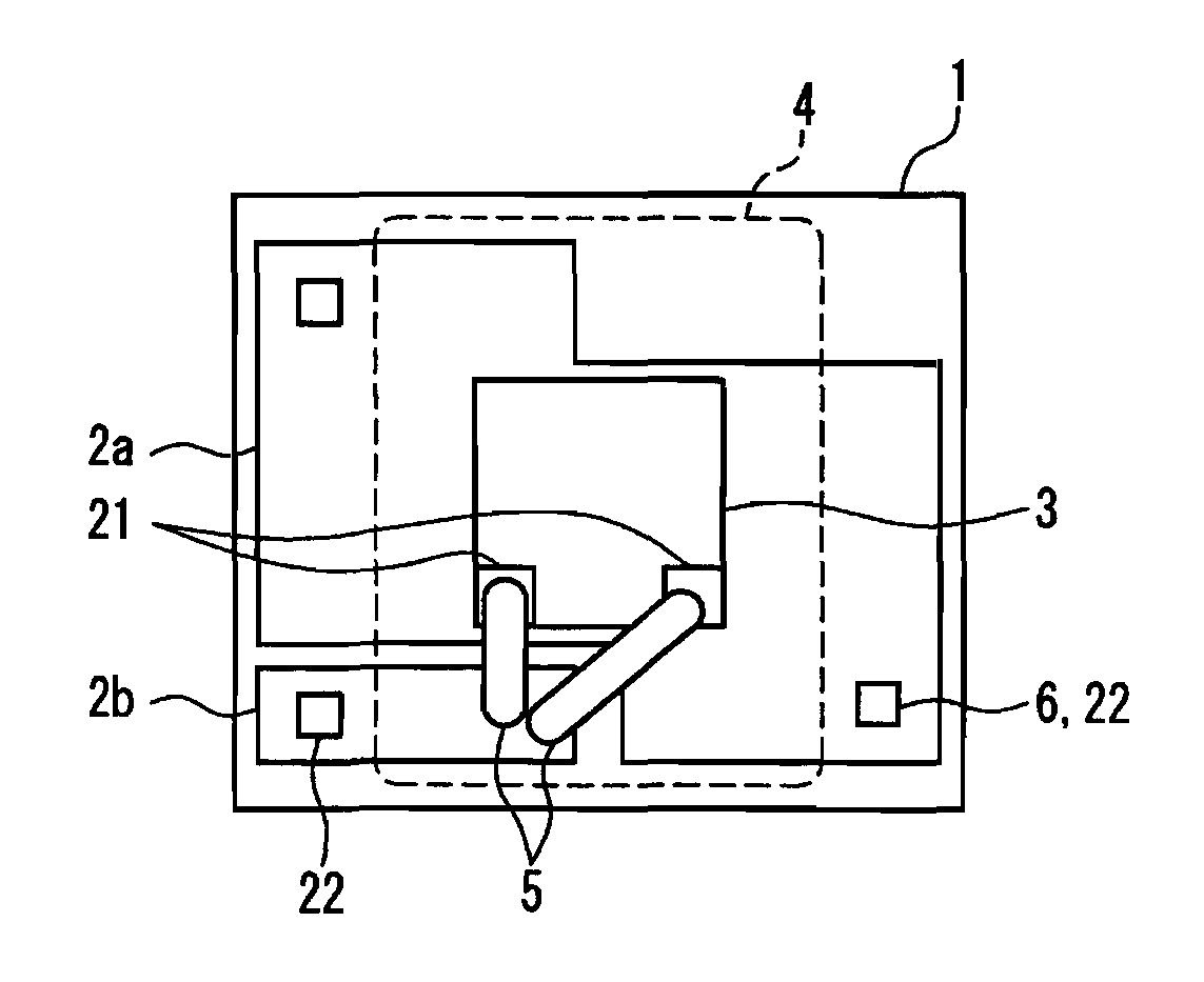
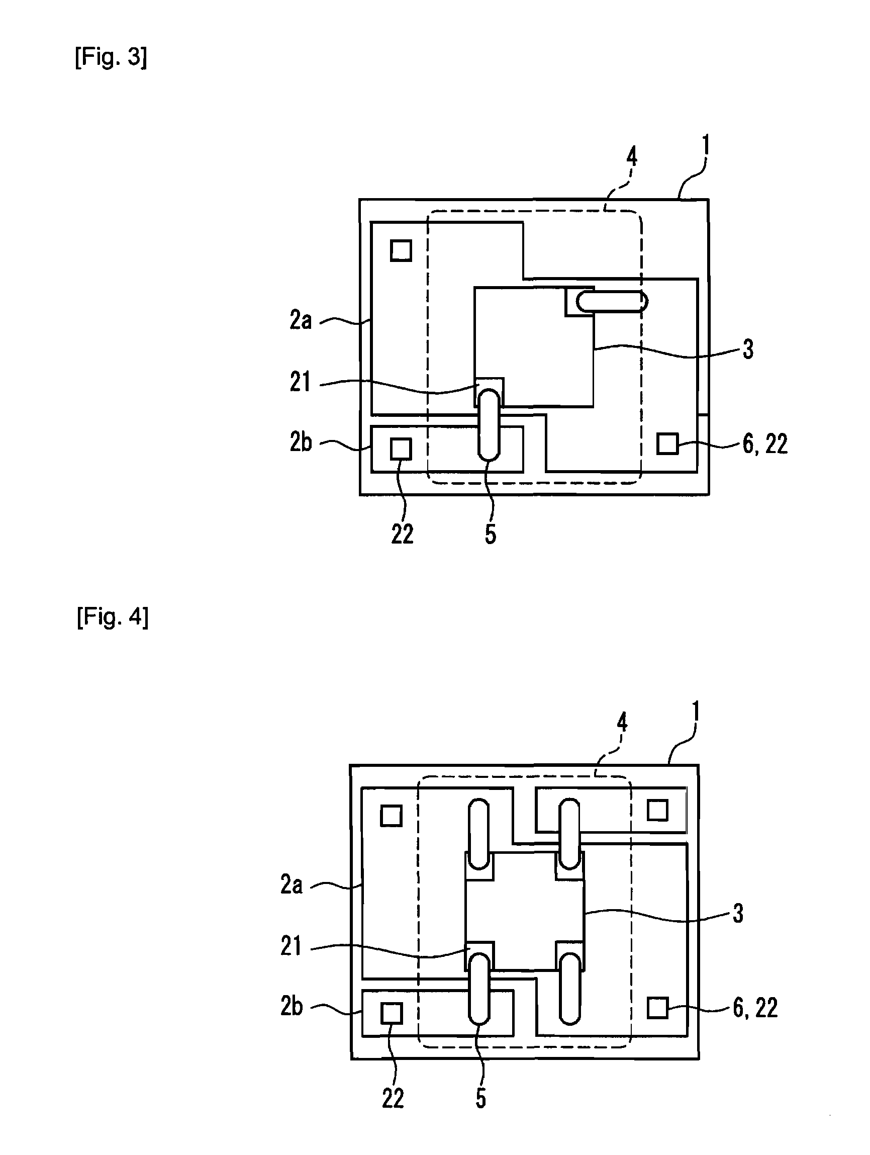
[0356]FIGS. 1 to 8 show top views showing semiconductor light-emitting devices according to Embodiment 1 of the present invention. The cross section taken on line I—I′ shown in FIG. 1 will be described later from Embodiment 3 onwards.

[0357](Pattern Forms of Conductor a 2a, Conductor B 2B, and Conductors X)

[0358]As shown in FIGS. 1 to 8, Embodiment 1 of the semiconductor light-emitting device according to the present invention includes at least one conductor A 2a, a conductor B 2b, and a solid-state light-emitting element 3 on one side of an insulating heat dissipating substrate 1, and the solid-state light-emitting element 3 is mounted on the conductor A 2a but is not mounted on the conductor B 2b. Embodiment 1 is characterized as follows. The solid-state light-emitting element 3 has a pair of a power supply electrode A 14a and a power supply el...

embodiment 2

[0414]The semiconductor light-emitting device of the present invention can include a plurality of at least conductors A 2a on one flat surface of the heat dissipating substrate 1 in the semiconductor light-emitting device of Embodiment 1. This makes it possible to include a plurality of solid-state light-emitting elements 3 and to increase the output power substantially in proportion to the number of the solid-state light-emitting elements 3.

[0415]Furthermore, as described above, a plurality of solid-state light-emitting elements 3 can be disposed in close proximity, by utilizing the shape with no line symmetry of the conductor A 2a, so that it becomes possible to mount a plurality of solid-state light-emitting elements 3 with high density.

[0416]Examples thereof are shown in FIGS. 12 to 16. The details of the respective components and outline of the operational effects are as described above in Embodiment 1 and other sections and therefore the details thereof are not repeated here. ...

embodiment 3

[0441]Hereinafter, for example, the arrangement of the solid-state light-emitting elements 3 is described in further detail.

[0442]FIG. 26 shows a cross section (side face) taken on line I-I′ shown in FIG. 1 of the semiconductor light-emitting device according to Embodiment 1 shown in FIG. 1 as an example.

[0443]In FIG. 26, the wavelength converter 4 is not shown. The arrangement of the wavelength converter 4 will be described in Embodiment 4.

[0444]As shown in FIG. 26 as a specific example, the semiconductor light-emitting device of the present invention includes at least one conductor A 2a, a conductor B 2b, and a solid-state light-emitting element 3 on one side of an insulating heat dissipating substrate 1. The solid-state light-emitting element 3 is mounted on (fixed onto) the conductor A 2a but is not mounted on the conductor B 2b. The semiconductor light-emitting device is characterized as follows. The solid-state light-emitting element 3 has a pair of power supply electrodes eit...


PUM


Abstract

A semiconductor light-emitting device of the present invention includes at least one conductor A, that is patterned electrode, 2a, a conductor B, that is patterned electrode, 2b, and a solid-state light-emitting element 3 on one side of an insulating heat dissipating substrate 1. The solid-state light-emitting element 3 is mounted on the conductor A 2a but is not mounted on the conductor B 2b. The solid-state light-emitting element 3 is mounted in such a manner that the whole lower surface that is a surface opposing to a main light extraction surface of the solid-state light-emitting element 3 adheres to the conductor A 2a. When a mounting surface of the solid-state light-emitting element 3 is viewed from above, the conductor A 2a has an element mounting area on which the whole lower surface of the solid-state light-emitting element 3 is mounted and a plurality of outflow-adhesive capturing areas that are provided adjacent to the periphery of the element mounting area without directional bias with respect to the periphery of the element mounting area. The conductor B 2b is disposed in a portion adjacent to the periphery of the element mounting area other than the outflow-adhesive capturing areas while being electrically separated from the conductor A 2a. In this manner, a semiconductor light-emitting device can be provided that can be produced using orthodox practical techniques, can have high output power, can be mounted with high density, and can be designed with consideration given to the case of lighting failures.

Description

TECHNICAL FIELD[0001]The present invention relates to all-solid-state semiconductor light-emitting devices that can be produced using highly proven practical techniques and that have high output power and can be mounted with high density, and to light source devices and lighting systems including the same.BACKGROUND ART[0002]Conventionally, a semiconductor light-emitting device has been known that includes a patterned wiring conductor, a solid-state light-emitting element, and a wavelength converter on a heat dissipating substrate, with the wavelength converter emitting light with a longer wavelength than that of primary light emitted by the solid-state light-emitting element through excitation by the primary light.[0003]An example of such a semiconductor light-emitting device is a light source that is known as a white LED. Various light source devices and lighting systems that include such semiconductor light-emitting devices have been proposed (see, for example, Patent Literatures...

Claims


Application Information

Patent Timeline
Patent Type & Authority Applications(United States)
IPC IPC(8): H05B39/06H01L33/00H01L33/50H01L33/62H01L33/64
CPCH01L25/0753H01L2224/45144H01L33/62H01L33/642H01L33/647H01L2224/48091H01L2224/73265H01L2924/09701H01L33/50H01L2224/49113H01L2924/01019H01L2924/01021H01L2924/01055H01L2924/01066H01L2924/01067H01L2924/01068H01L2224/32225H01L2224/48227H01L2924/07802H01L24/45H01L2924/3025H01L2924/00014H01L2924/00H01L2924/00012H01L2924/12044H01L2924/12041H01L24/73H01L2924/181
Inventor OSHIO, SHOZOTANIMOTO, NORIYASU
Owner PANASONIC CORP
Learn More