Methods and apparatus for reducing coupling in a mos device

a technology of mos device and coupling, applied in the field of mos device layout, can solve the problems of weaker parasitic coupling and significantly weaker parasitic coupling, and achieve the effect of reducing capacitan

Active Publication Date: 2010-07-22
STMICROELECTRONICS SRL
View PDF12 Cites 24 Cited by
  • Summary
  • Abstract
  • Description
  • Claims
  • Application Information

AI Technical Summary

Problems solved by technology

However, this parasitic coupling becomes significantly weaker at further distances (i.e., the further the metallization layer is from the gate 108, the weaker the parasitic coupling will be).

Method used


Image

  • Methods and apparatus for reducing coupling in a mos device
  • Methods and apparatus for reducing coupling in a mos device
  • Methods and apparatus for reducing coupling in a mos device

Examples


Embodiment Construction

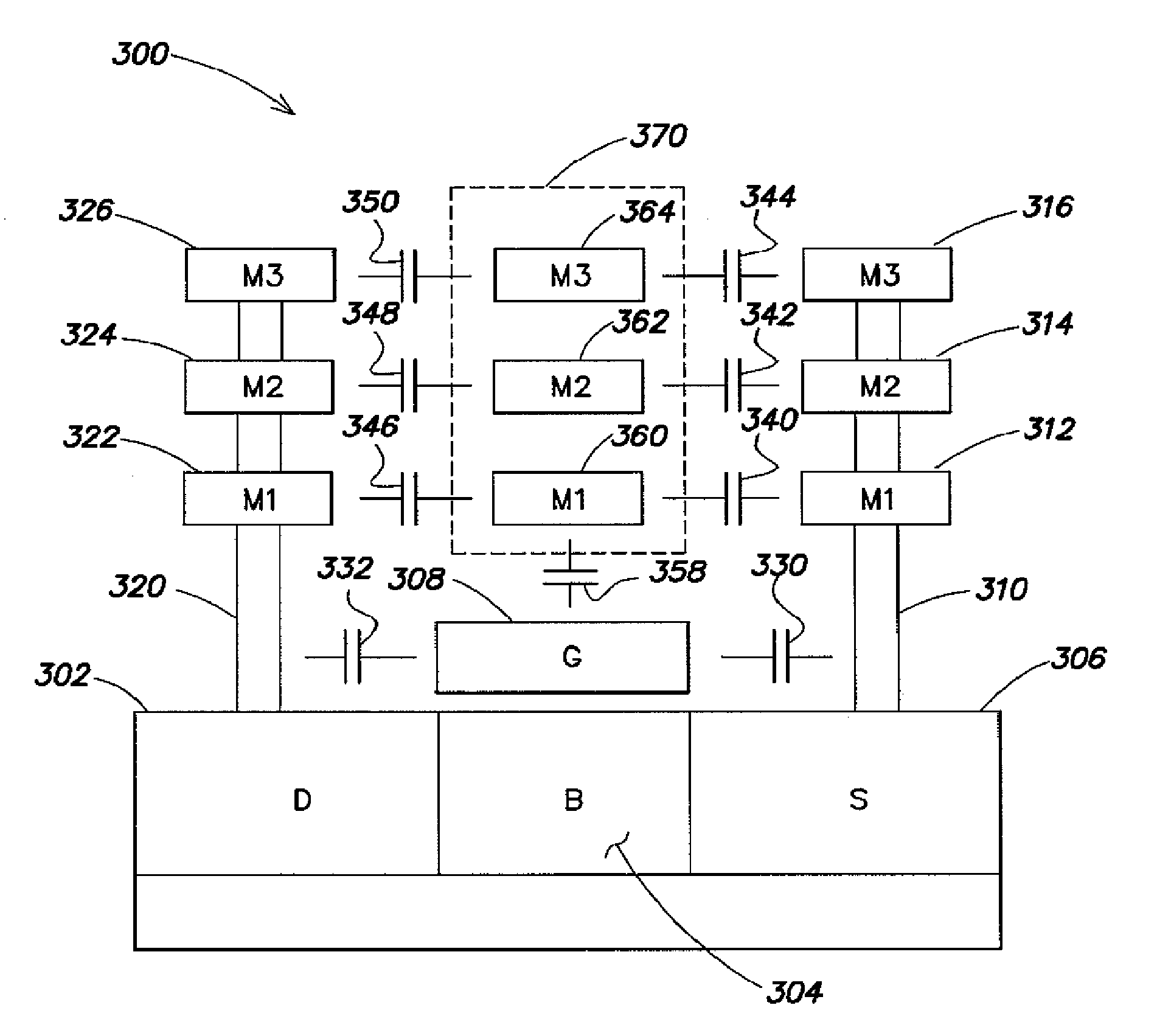
[0022]Embodiments of the present invention relate to a shielding structure for a MOS device to reduce at least some coupling between the terminals of the MOS device. The incorporation of a shielding structure above the gate of a MOS device as disclosed herein, reduces the coupling between terminals of the device to realize a MOS device with increased switching times despite reduced dimensions, and that may be suitable in some low-power applications

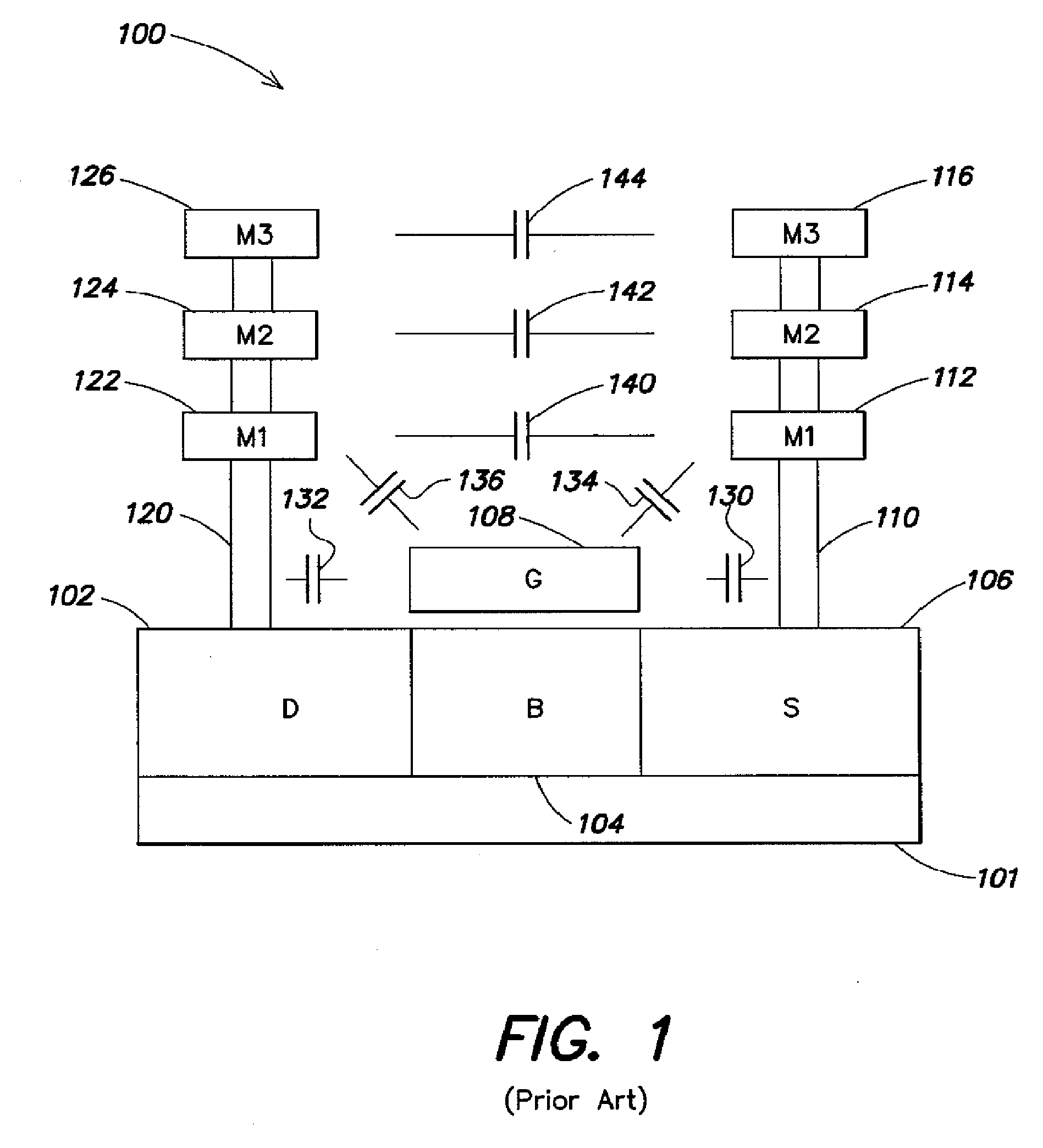
[0023]Applicants have recognized and appreciated that as the dimensions of a MOS device become smaller, the coupling between the regions of a MOS device become more problematic (i.e., the coupling increases) as the distances between the components of the device decreases. Thus, according to some embodiments of the invention, a shielding structure is provided above the gate of a MOS device to reduce at least some of the coupling between the regions of the device.

[0024]An embodiment of the invention is illustrated schematically in FIG. 3. In...


PUM


Abstract

Mutual capacitances between regions of a MOS device become substantial factors that limit the speed and performance of the device as the device dimensions are reduced in size. A MOS transistor with a shielding structure formed above the gate is described. The shielding structure is connected to ground and is configured to reduce at least some of these mutual capacitances.

Description

BACKGROUND OF THE INVENTION[0001]1. Field of the Invention[0002]The present invention relates generally to semiconductor design, and more specifically to a MOS layout with reduced coupling between the terminals of the MOS device.[0003]2. Discussion of the Related Art[0004]Metal-oxide semiconductor field effect transistors (MOSFETs) are used as discrete devices and as active elements in digital and analog integrated circuits (ICs) for a variety of applications ranging from microprocessors and memory to communications devices. A block diagram representation of a cross-sectional view of a conventional MOS structure is illustrated in FIG. 1. The semiconductor portion of the MOS structure 100 includes a drain region 102, a channel region (bulk) 104, and a source region 106. MOSFETs can be either n-channel or p-channel devices. In an n-channel MOSFET, the substrate 101 is a p-type semiconductor (e.g., silicon) and the drain region 102 and the source region 106 are n+ doped regions. MOSFET...

Claims


Application Information

Patent Timeline
Patent Type & Authority Applications(United States)
IPC IPC(8): H03H11/24H01L21/28H01L29/78
CPCH01L23/5225H01L2924/3011H01L2924/0002H01L29/78H01L2924/00
Inventor CANTONI, ADALBERTO
Owner STMICROELECTRONICS SRL
Why Eureka
Try Eureka