Unlock instant, AI-driven research and patent intelligence for your innovation.

Semiconductor package and manufacturing method thereof

Inactive Publication Date: 2010-08-26
YAMAHA CORP
View PDF19 Cites 0 Cited by
  • Summary
  • Abstract
  • Description
  • Claims
  • Application Information

AI Technical Summary

Benefits of technology

[0009]It is an object of the present invention to provide a semiconductor package which simplifies plating on the backside of a stage with its surface mounting a semiconductor chip thereon and which prevents plating from being taken away.
[0011]When a plurality of semiconductor packages is vertically assembled, the protrusion formed on the upper surface of the outer portion of the resin mold of the lower semiconductor package is brought into contact with the lower surface of the outer portion of the resin mold of the upper semiconductor package, or the protrusion formed on the lower surface of the outer portion of the resin mold of the upper semiconductor package is brought into contact with the upper surface of the outer portion of the resin mold of the lower semiconductor package. Thus, a gap corresponding to the protrusion is formed between the exposed backside of the stage of the upper semiconductor package and the upper surface of the resin mold of the lower semiconductor package. Due to such a gap, it is possible to reliably prevent the exposed backside of the stage of the upper semiconductor package from coming in contact with the upper surface of the resin mold of the lower semiconductor package, thus preventing the plating applied to the backside of the stage from being taken away.
[0012]Due to the formation of the protrusion, the present invention does not needs a conventional spacer interposed between vertically adjacent semiconductor packages. This simplifies plating applied to the backside of the stage of each semiconductor package, thus improving the manufacturing efficiency of semiconductor packages.
[0013]When a plurality of semiconductor packages is vertically assembled after plating, it is possible to prevent the plating applied to the backside of the stage of the upper semiconductor package from being struck to the upper surface of the resin mold of the lower semiconductor package.

Problems solved by technology

Interposing spacers between semiconductor packages is troublesome and is likely to reduce the manufacturing efficiency of semiconductor packages.

Method used


Image

  • Semiconductor package and manufacturing method thereof
  • Semiconductor package and manufacturing method thereof
  • Semiconductor package and manufacturing method thereof

Examples


Embodiment Construction

[0027]The present invention will be described in further detail by way of examples with reference to the accompanying drawings.

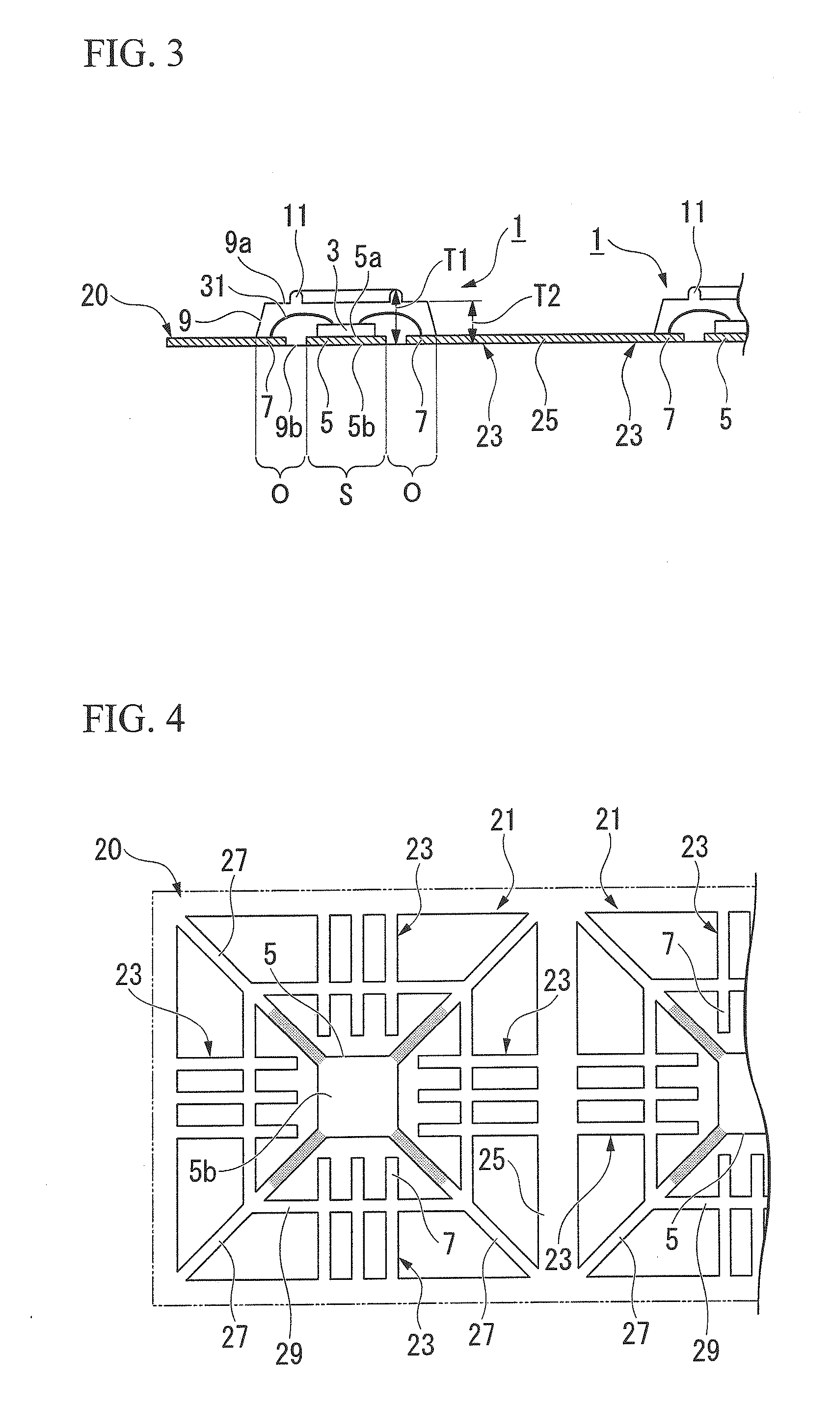
[0028]A semiconductor package 1 according to a preferred embodiment of the present invention will be described with reference to FIGS. 1 to 5. A plurality of semiconductor packages (each corresponding to the semiconductor package 1 of the present embodiment) is unified to adjoin together via a thin metal plate 20 and is then divided into individual pieces in the final stage of manufacturing.

[0029]As shown in FIGS. 1 to 3, the semiconductor package 1 is constituted of a semiconductor chip 3, a rectangular-shaped stage 5 with a surface 5a mounting the semiconductor chip 3 thereon, a plurality of inner leads 7 which are disposed in the periphery of the semiconductor chip 3 and are electrically connected to the semiconductor chip 3, and a resin mold 9 which seals the semiconductor chip 3, the stage 5, and the inner leads 7 therein.

[0030]The stage 5 and the inner...


PUM


Abstract

A semiconductor package is constituted of a semiconductor chip, a rectangular-shaped stage having the semiconductor chip mounted on the surface, a plurality of leads which are aligned in the periphery of the stage and which are electrically connected to the semiconductor chip, and a resin mold which seals the semiconductor chip, the stage, and the leads therein while externally exposing the backside of the stage on the lower surface thereof. In particular, at least one protrusion is further formed on the upper surface or the lower surface of the resin mold at a position within the outer portion of the resin mold disposed outside the sealed portion of the resin mold. The height of the outer portion of the resin mold having the protrusion is larger than the sum of the thickness of the stage and the thickness of the sealed portion of the resin mold.

Description

BACKGROUND OF THE INVENTION[0001]1. Field of the Invention[0002]The present invention relates to semiconductor packages that encapsulate semiconductor chips mounted on stages of lead frames sealed with resin molds. The present invention also relates to manufacturing methods of semiconductor packages.[0003]The present application claims priority on Japanese Patent Application No. 2009-38319, the content of which is incorporated herein by reference.[0004]2. Description of the Related Art[0005]Various semiconductor packages have been developed and disclosed in various documents such as Patent Document 1. In semiconductor packages, semiconductor chips are mounted on the surfaces of rectangular-shaped stages of lead frames sealed with resin molds. For the purpose of efficiently dissipating heat from semiconductor chips, the backsides of stages are not sealed with resin molds but are exposed externally. In semiconductor packages, plating is applied to the backsides of stages so as to impr...

Claims


Application Information

Patent Timeline
IPC IPC(8): H01L23/495H01L21/56
CPCH01L23/3107H01L23/49582H01L2224/48245H01L2924/1815H01L2224/48247H01L24/97H01L24/48H01L2924/181H01L2224/48091H01L2924/00014H01L2924/00012H01L2224/45099H01L2224/45015H01L2924/207
Inventor FUKUDA, YOSHIO
Owner YAMAHA CORP
Features
  • R&D
  • Intellectual Property
  • Life Sciences
  • Materials
  • Tech Scout
  • Unparalleled Data Quality
  • Higher Quality Content
  • 60% Fewer Hallucinations
Learn More