

Image processing device, image processing method, and imaging device
a technology of image processing and image processing method, which is applied in the field of image processing device, image processing method, imaging device, etc., can solve the problems of insufficient color component sensitivity level value accuracy, interpolation is impacted, accuracy further deterioration,
- Summary
- Abstract
- Description
- Claims
- Application Information
AI Technical Summary
Problems solved by technology
Method used
Image



Examples
first embodiment
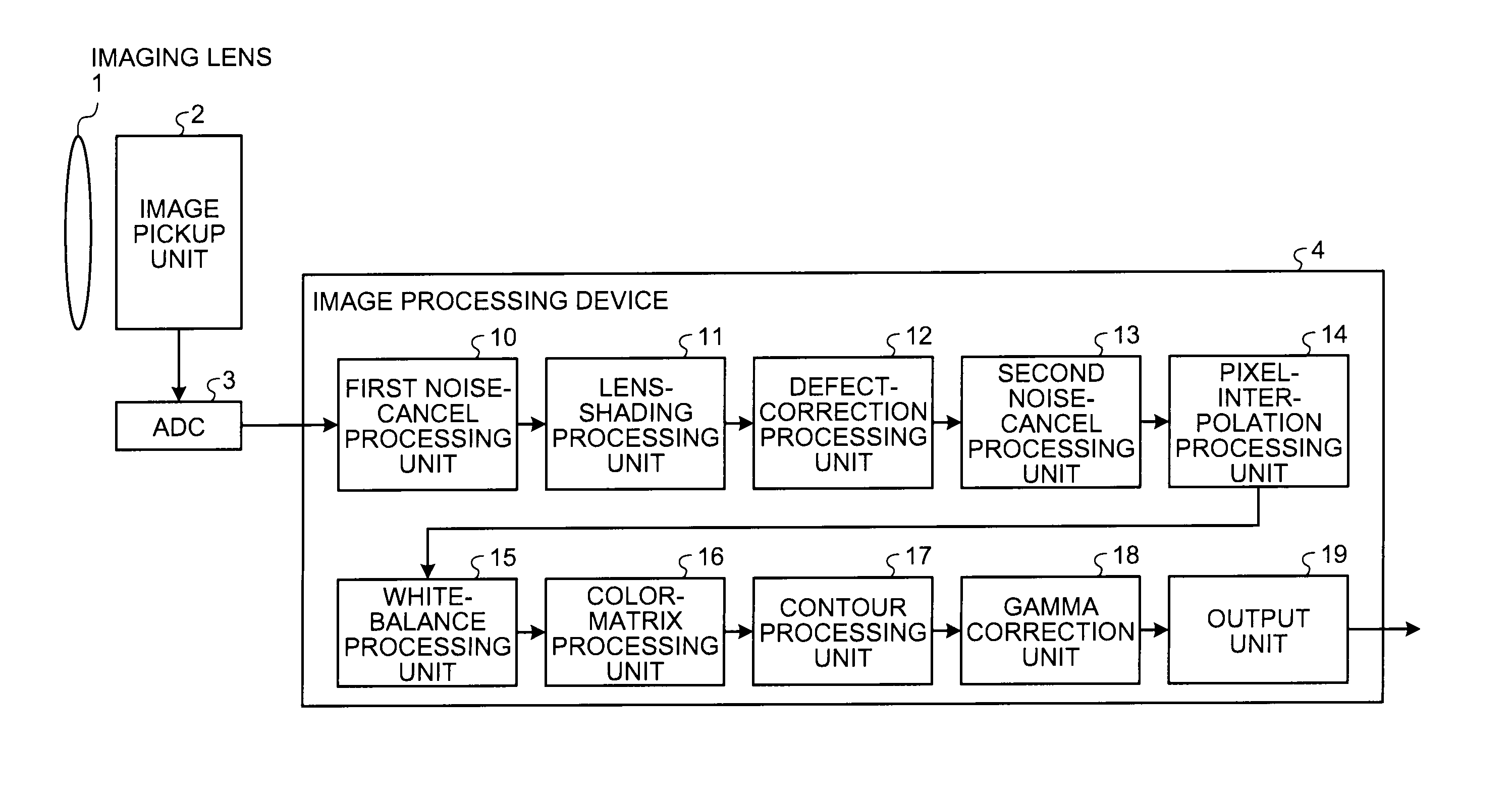
[0030]FIG. 1 is a block diagram of a solid-state imaging device as an imaging device according to the present invention. The solid-state imaging device includes an imaging lens 1, an image pickup unit 2, an analog-digital converter (ADG) 3, and an image processing device 4. The imaging lens 1 captures light from a subject. The image pickup unit 2 coverts the light from the subject into a signal charge to thereby pick up a subject image. The image pickup unit 2 captures pixel values of red, blue, and green in order corresponding to the Bayer array, sequentially amplifies captured analog image signals with a gain corresponding to an imaging condition designated from the outside, and outputs the analog image signals. The ADC 3 converts the analog image signals output from the image pickup unit 2 into digital image signals. The image processing device 4 applies various kinds of image processing to the digital image signals output from the ADC 3.
[0031]The image processing device 4 includ...
second embodiment
[0064]the present invention is characterized in that pixels for G are classified into Gr pixels and Gb pixels and interpolated sensitivity level values by interpolation of the Gr pixels and interpolation sensitivity level values by interpolation of the Gb pixels are calculated. The Gr pixels are first pixels for green located in rows in which pixels for R are arrayed in parallel in the H direction among the pixels for G. The Gb pixels are second pixels for green located in rows in which pixels for B are arrayed in parallel in the H direction. The Gr pixels are pixels for G having the same form of arrays in two-dimensional directions because the Gr pixels are adjacent to the pixels for R in the H direction. The Gb pixels are pixels for G having the same form of arrays in the two-dimensional directions because the Gb pixels are adjacent to the pixels for B in the H direction.
[0065]FIG. 16 is a diagram for explaining calculation of interpolated sensitivity level values performed when a...
third embodiment
[0069]the present invention is characterized in that sensitivity level values of G components are respectively corrected for a pixel Gr0 and a pixel Gb0 according to interpolated sensitivity level values by interpolation of Gr pixels and interpolated sensitivity level values by interpolation of Gb pixels. This embodiment is explained below with reference to FIGS. 16 and 17.
[0070]The arithmetic unit for G 21G (se FIG. 14) calculates a predetermined ratio of interpolated sensitivity level values generated by interpolation using Gr1, Gr2, Gr3, and Gr4 and interpolated sensitivity level values generated by interpolation using Gb1, Gb2, Gb3, and Gb4. The arithmetic unit for G 21G corrects, with the calculated predetermined ratio set as a parameter, a sensitivity level value of the G component in the pixel Gr0 and a sensitivity level value of the G component in the pixel Gb0.
[0071]When an output difference occurs between a Gr pixel and a Gb pixel, color reproducibility falls because a dif...
PUM
 Abstract
Description
Claims
Application Information