Field effect transistor gate process and structure

a field effect transistor and gate technology, applied in the field of field effect transistors and metalsemiconductor field effect transistors, can solve the problems of limiting the operation of the transistor or the reliability or both

Inactive Publication Date: 2010-09-30
NXP USA INC
View PDF7 Cites 6 Cited by
  • Summary
  • Abstract
  • Description
  • Claims
  • Application Information

AI Technical Summary

Problems solved by technology

Despite their great utility, FET devices of various kinds continue to suffer from a number of problems which limit their operating properties or reliability or both.

Method used


Image

  • Field effect transistor gate process and structure
  • Field effect transistor gate process and structure
  • Field effect transistor gate process and structure

Examples


first embodiment

[0026] there is provided a method for forming a metal-semiconductor field effect transistor (MESFET) (20′, 20″), comprising, providing a substrate (21) having a mask layer (43) thereon with an opening (51) extending to a surface region (291) of the substrate (21), etching a gate recess (36) in the surface region (291) of the substrate (21) so as to expose a depressed surface (362) of the substrate (21) and also form surface undercut cavities (363) extending laterally under the mask layer (43) from the gate recess (36), and substantially conformally coating the depressed surface (362) and inner surfaces (366) of the surface undercut cavities (363) with a Schottky forming conductor (40′), thereby forming a Schottky gate contact (271) to the substrate (21), adapted when biased to control current flow in a channel (22) underlying the gate recess (36). According to a further embodiment, the method further comprises forming a conformal or non-conformal barrier layer conductor (41′, 41″) o...

second embodiment

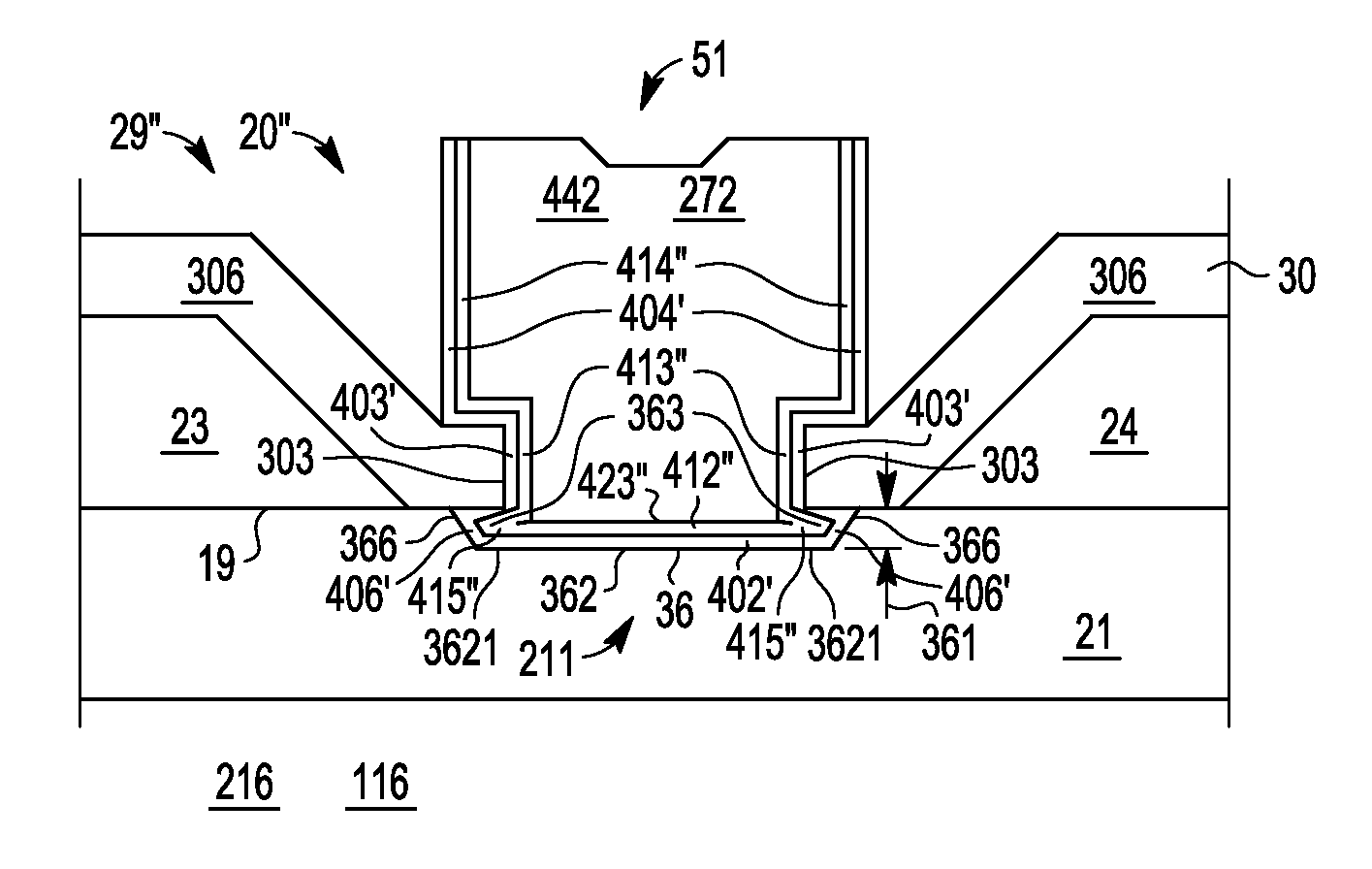
[0027] there is provided a metal-semiconductor field effect transistor (MESFET) (20′, 20″), comprising, a semiconductor substrate (21) having a gate region (29′, 29″) in which is located a surface portion (362) of the substrate (21) bordered by lateral undercut regions (363), and a Schottky contact forming conductor (40′) overlying the surface portion (362) of the substrate (21) and on sidewalls (366) of the undercut regions (363). According to a still further embodiment, the undercut regions (363) have a first depth (361) substantially perpendicular to the surface portion (362) and the Schottky forming conductor (40′) has a first thickness (401′, 4021′) substantially perpendicular to the surface portion (362) and wherein the first thickness (401′, 4021′) is 30% to 80% of the first depth (361). According to a yet further embodiment, the substrate comprises a III-V material. According to a still yet further embodiment, the surface portion (362) is located in a recess (36) in the subs...

third embodiment

[0028] there is provided a method for forming a gate conductor (27) of a metal-semiconductor field effect transistor (MESFET), comprising, providing a substrate (21) having a semiconductor first surface (291), applying a mask (43) having an opening (51) above the semiconductor first surface (291), etching the semiconductor first surface (291) through the opening (51) substantially vertically to a first depth (361) thereby exposing an interior surface (362) of the substrate (21) and substantially laterally underneath edges (303) of the mask (43) adjacent the opening (51) to a first distance (364), thereby forming a recess (36) having the interior surface (362) and lateral undercut regions (363) with sidewalls (366, 3521) shadowed by the edges (303) of the mask (43), and conformally depositing a Schottky forming conductor (40′) of a first thickness (401′, 4021′) on the interior surface (362) and on the sidewalls (366, 3621) of the undercut regions (363). According to a further embodim...


PUM


Abstract

A Schottky gate (27′, 27″) of a metal-semiconductor FET (20′, 20″) is formed on a semiconductor comprising substrate (21) by, etching a gate recess (36) so as to expose a slightly depressed surface (362) of the substrate (21), the etching step also producing surface undercut cavities (363) extending laterally under the etch mask (43) from the gate recess (36), then conformally coating the slightly depressed surface (362) with a first Schottky forming conductor (40′) and substantially also coating inner surfaces (366) of the surface undercut cavities (363), and forming a Schottky contact to the semiconductor comprising substrate (21), adapted when biased to control current flow in a channel (22) extending between source (23) and drain (24) of the FET (20′, 20″) under the gate recess (36). In further embodiments, a conformal or non-conformal barrier layer conductor (41′, 41″) may be provided over the Schottky forming conductor (40′) and a thicker overlying gate conductor (442, 272) provided over the barrier layer conductor (41′, 41″).

Description

FIELD OF THE INVENTION[0001]The present invention generally relates to electronic devices, more particularly, field effect transistors (FETs), especially metal-semiconductor field effect transistors (MESFETs).BACKGROUND OF THE INVENTION[0002]Metal-semiconductor field effect transistors (MESFETs) are much used in modern day electronics, especially high frequency devices employing binary or ternary III-V semiconductors. GaAs, AlGaAs, InGaAs, AlInAs, and other combinations are non-limiting examples of materials commonly used in such devices. Such combination of semiconductor epitaxial layers can create devices with high electron mobility and are often referred to as high electron mobility transistors (HEMT), pseudomorphic high electron mobility transistors (PHEMT) or metamorphic high electron mobility transistor (MHEMT).[0003]FIG. 1 shows a simplified schematic cross-sectional view through generalized MESFET device 20, 20′, 20″ comprising, semiconductor containing substrate 21 extendin...

Claims


Application Information

Patent Timeline
Patent Type & Authority Applications(United States)
IPC IPC(8): H01L29/812H01L21/338
CPCH01L21/28587H01L29/20H01L29/8128H01L29/778H01L29/66856
Inventor HUANG, JENN HWA
Owner NXP USA INC
Why Eureka
Try Eureka