Display device, and methods for manufacturing and controlling the display device

a display device and display technology, applied in the manufacture of electric discharge tubes/lamps, lighting and heating apparatuses, instruments, etc., can solve the problems of increasing manufacturing costs, affecting the accuracy of measurement results, and requiring long accumulation time to perform plural measurements, so as to reduce the amount of data, reduce manufacturing costs and driving processing load, and reduce manufacturing costs. the effect of significant reduction of manufacturing costs

Active Publication Date: 2010-10-07
JOLED INC
View PDF9 Cites 26 Cited by
  • Summary
  • Abstract
  • Description
  • Claims
  • Application Information

AI Technical Summary

Benefits of technology

[0016]In contrast to the electric current program pixel circuit which determines light emission luminance by applying a data current from outside, the application is given for correcting uneven luminance in each pixel in the data voltage application type pixel circuit which determines light emission luminance by applying a data voltage from outside. However, in the data voltage application type pixel circuit, the luminance correction data of each pixel is not uniquely determined by only measuring the luminance ratio of each pixel with respect to the same voltage using one kind of input tone, based on the non-linear relational characteristics between the input voltages and the luminance values. In order to calculate luminance correction data of each pixel applicable in a necessary input tone range, at least two kinds of input tones are required in the measurement. In this case, even when it takes not so much time to perform one measurement of an input voltage and a luminance using one kind of input tone, it takes long accumulation time to perform plural measurements. This increases the manufacturing cost, and requires complex correction processing in the light emission driving.
[0032]For this, it is possible to significantly reduce the amount of data required to correct various luminance of the respective pixel units of the display panel to obtain video signals having luminance common throughout the display screen. Thereby, the manufacturing cost can be reduced significantly. As the result, it is possible to reduce the manufacturing cost and the driving processing load, and achieve uniform display throughout the display screen.

Problems solved by technology

Thus, compensation for uneven luminance which is executed while keeping a correction accuracy entails a problem of an increase in the manufacturing cost.
Further, the time to measure the whole panel increases as the panel size or the number of input tones increases, which places a significant burden on the manufacturing cost.
However, in the data voltage application type pixel circuit, the luminance correction data of each pixel is not uniquely determined by only measuring the luminance ratio of each pixel with respect to the same voltage using one kind of input tone, based on the non-linear relational characteristics between the input voltages and the luminance values.
In this case, even when it takes not so much time to perform one measurement of an input voltage and a luminance using one kind of input tone, it takes long accumulation time to perform plural measurements.
This increases the manufacturing cost, and requires complex correction processing in the light emission driving.

Method used


Image

  • Display device, and methods for manufacturing and controlling the display device
  • Display device, and methods for manufacturing and controlling the display device
  • Display device, and methods for manufacturing and controlling the display device

Examples


embodiment 1

[0083]Embodiments of the present invention are described below with reference to the drawings.

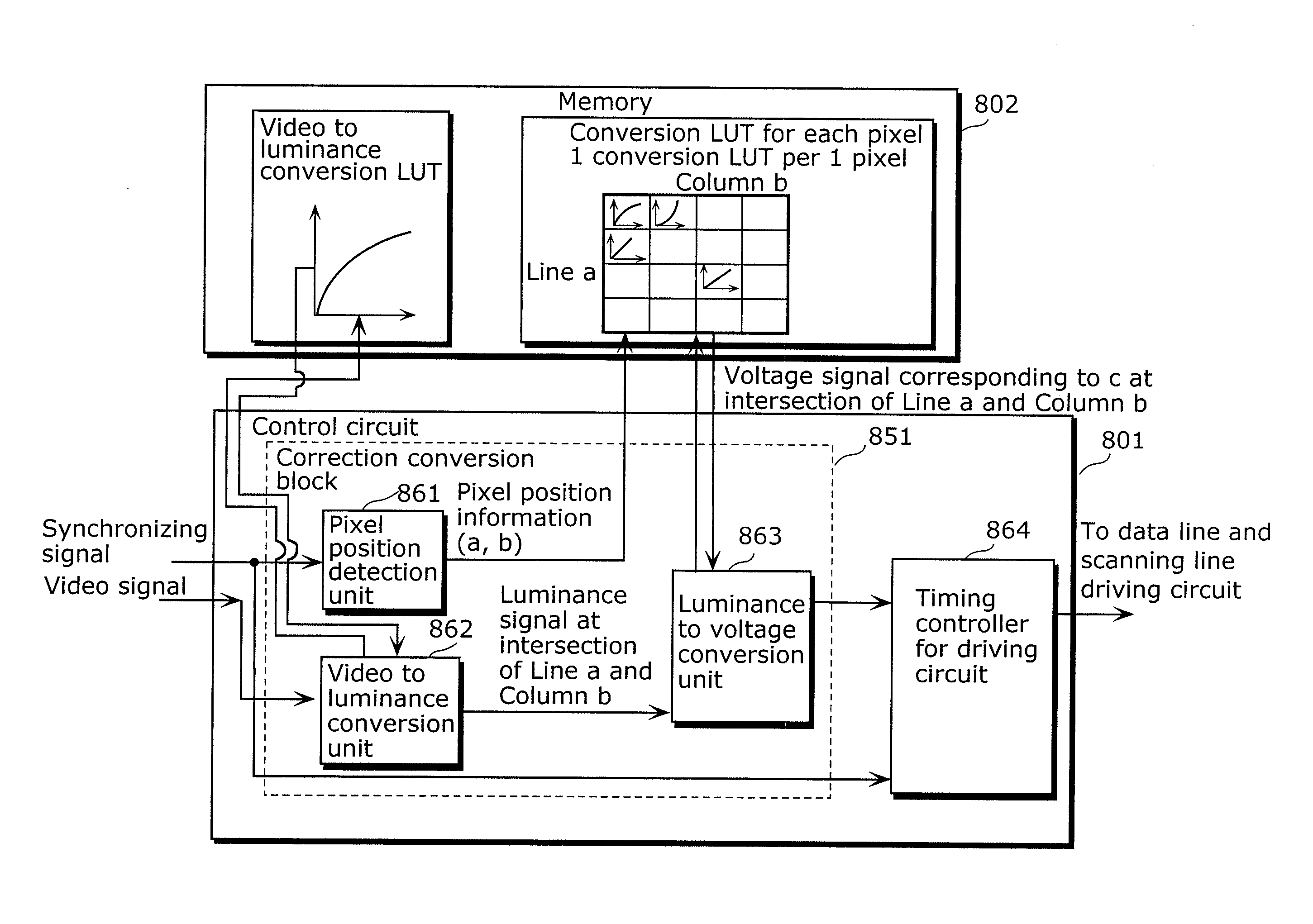
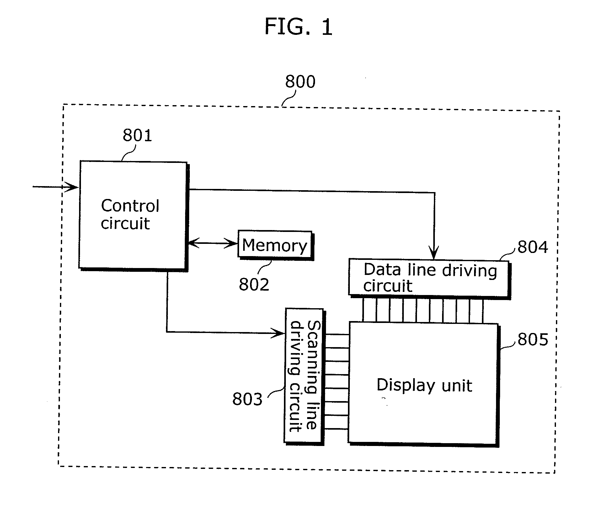
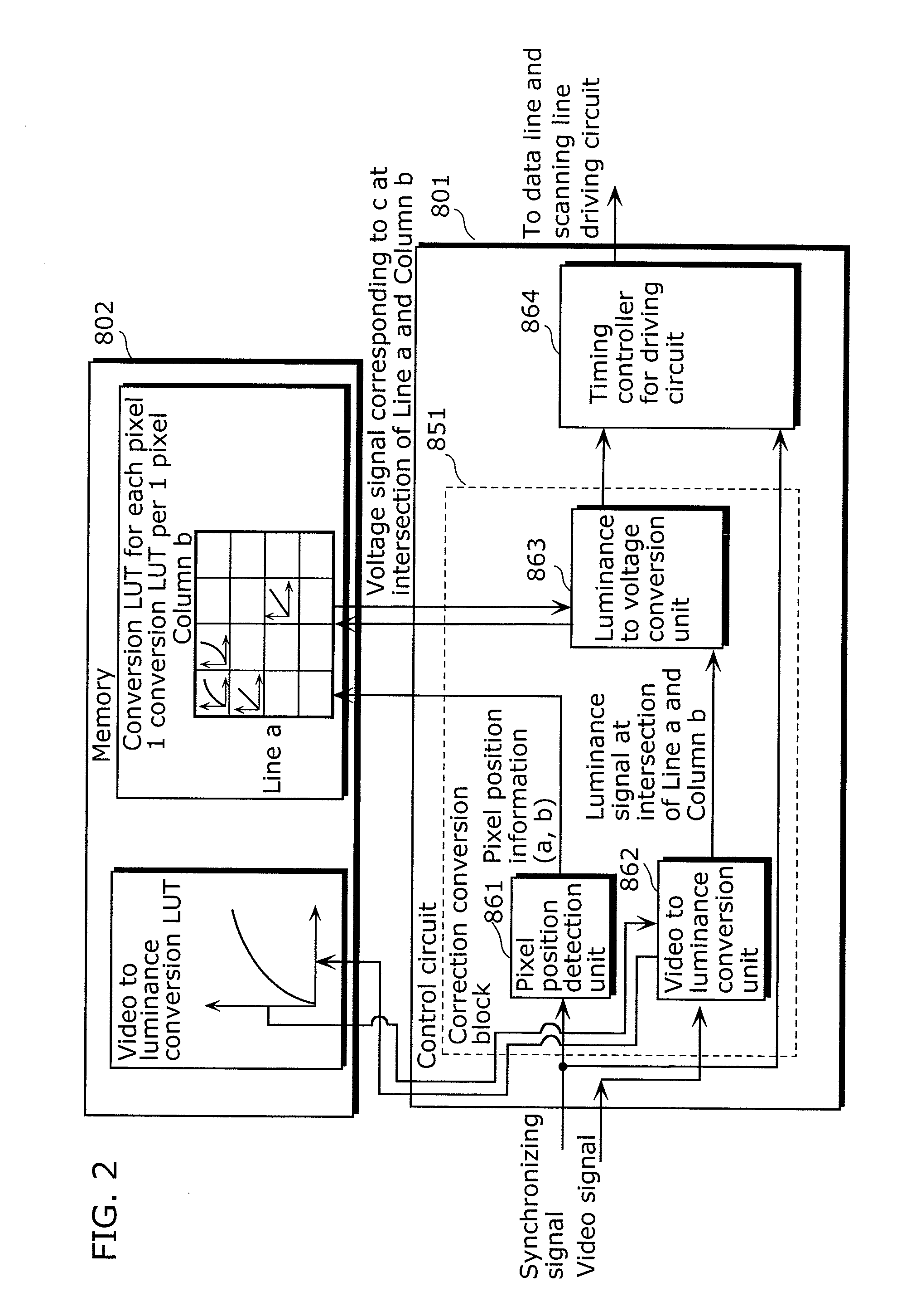
[0084]FIG. 3 is a block diagram showing an electric structure of a display device 100 according to Embodiment 1 of the present invention. A display device 100 in the diagram includes a control circuit 101, a memory 102, a scanning line driving circuit 103, a data line driving circuit 104, and a display unit 105.

[0085]The control circuit 101 has a function for controlling the memory 102, the scanning line driving circuit 103, and the data line driving circuit 104. The memory 102 stores a video to luminance conversion look up table (hereinafter referred to as a “video to luminance LUT”) used to convert a video signal into a luminance signal corresponding to the video signal, and a representative look up table (hereinafter referred to as a “representative LUT”) derived based on the representative conversion curve. The control circuit 101 reads characteristic parameters written in the memory 10...


PUM


Abstract

A display device corrects uneven luminance due to uneven element characteristics by simple measurement and correction with a low cost. The display device includes pixels that each include a light emitter and a driver. Data lines supply a voltage signal to the driver of each pixel. A data line driver supplies the voltage signal to each data line. A first memory stores, for each pixel, a luminance gain for adjusting a luminance corresponding to a video signal to a standard luminance. A second memory stores conversion curve information representing a representative conversion curve common to the pixels. A corrector converts, for each pixel, the luminance into a corresponding standard luminance value based on a corresponding luminance gain stored in the first memory, while a converter converts, for each pixel, the corresponding standard luminance into a corresponding voltage signal based on the conversion information stored in the second memory.

Description

CROSS REFERENCE TO RELATED APPLICATION[0001]This is a continuation application of PCT Application No. PCT / JP2009 / 002348 filed on May 28, 2009, designating the United States of America, the disclosure of which, including the specification, drawings, and claims, is incorporate herein by reference in its entirety.[0002]The disclosure of Japanese Patent Application No. 2008-139863 filed on May 28, 2008 including specification, drawings and claims is further incorporated herein by reference in its entirety.BACKGROUND OF THE INVENTION[0003]1. Field of the Invention[0004]The present invention relates to display devices and methods for manufacturing and controlling the display devices, and in particular to a display devices using a current-driven light emitting elements and methods for manufacturing and controlling the display devices.[0005]2. Description of the Related Art[0006]Image display devices in which organic EL elements (also known as organic light emitting diodes, or OLEDs) are us...

Claims


Application Information

Patent Timeline
Patent Type & Authority Applications(United States)
IPC IPC(8): G09G5/10H01J9/00
CPCG09G3/3233G09G2320/0285G09G2320/029G09G2320/0693G09G2320/045G09G2320/0673G09G2320/043G09G3/30G09G3/32
Inventor ODAWARA, RIEKATO, TOSHIYUKI
Owner JOLED INC
Why Eureka
Try Eureka