Electro-optic device, driving method thereof and electronic device

Inactive Publication Date: 2010-10-14
SEIKO EPSON CORP
View PDF0 Cites 2 Cited by
  • Summary
  • Abstract
  • Description
  • Claims
  • Application Information

AI Technical Summary

Benefits of technology

[0012]Further, another advantage of some aspects of the invention is that it provides an electro-optic device, a driving method thereof and an electronic device capable of addressing the problem associated with the electro-optic device, the driving method thereof and the electronic device of such an aspect.
[0029]As described above, according to this embodiment, the arrangement balance of the capacitor elements involved in discharging (and charging) is good with respect to the electro-optic elements to be driven, and even when any one of the plural electro-optic elements is emitted, occurrence of brightness unevenness and the like can be suppressed since the current supply condition is equal.
[0036]According this aspect, for example, since an operation of changing the control line to be selected for each one horizontal period is not required to be performed, in order to be capable of being realized in the last and the previous two aspects, reduction in power consumption and the like is possible.
[0039]According to the aspect, since the predetermined period is one vertical period, firstly, as described in the example, the number of times of the change operations is reduced compared with that the control lines to be selected is changed in every one horizontal period, so that the consumption power reduce effect is obtained. In addition, secondly, in this aspect, since the control line to be selected is changed in every one vertical period without performing the change operation at all, brightness unevenness reduce effect as described above, that is, brightness unevenness reduce effect such that the current supply condition can be equal with respect to the electro-optic elements is obtained also in this aspect.
[0042]Since the electronic device according to the invention includes various types of electro-optic devices described above, it is possible to easily adjust brightness of the whole image.
[0044]According to the embodiment of the invention, it is possible to appropriately drive the electro-optic device of the invention described above.

Problems solved by technology

However, the electro-optic device described above has the problems as follows.
However, due to the relationship in which a physical space to be allowed for each driving circuit, the large capacitance value is difficult to be implemented.
However, in the technique according to US Patent Application Publication No. 2009 / 0195534, since there is no emission control transistor as described above, the configuration and the method described above cannot be employed.

Method used


Image

  • Electro-optic device, driving method thereof and electronic device
  • Electro-optic device, driving method thereof and electronic device
  • Electro-optic device, driving method thereof and electronic device

Examples


first embodiment

[0065]Hereinafter, the first embodiment according to the invention will be described with reference to FIG. 1 and FIG. 2. In addition to FIG. 1 and FIG. 2 mentioned herein, in each of the drawings referred to below, the ratios of dimensions of each part may be properly different from the actual condition.

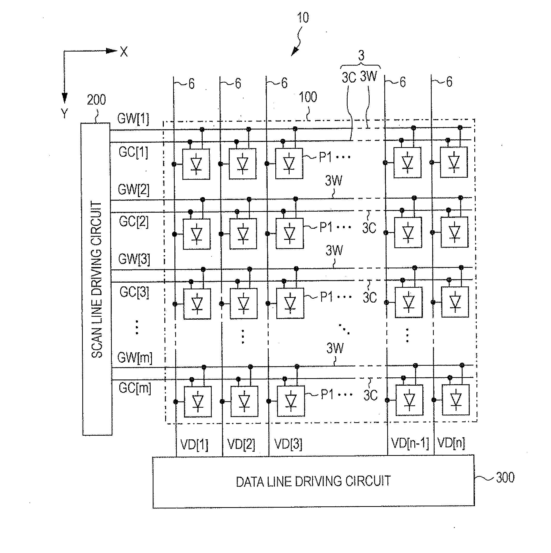
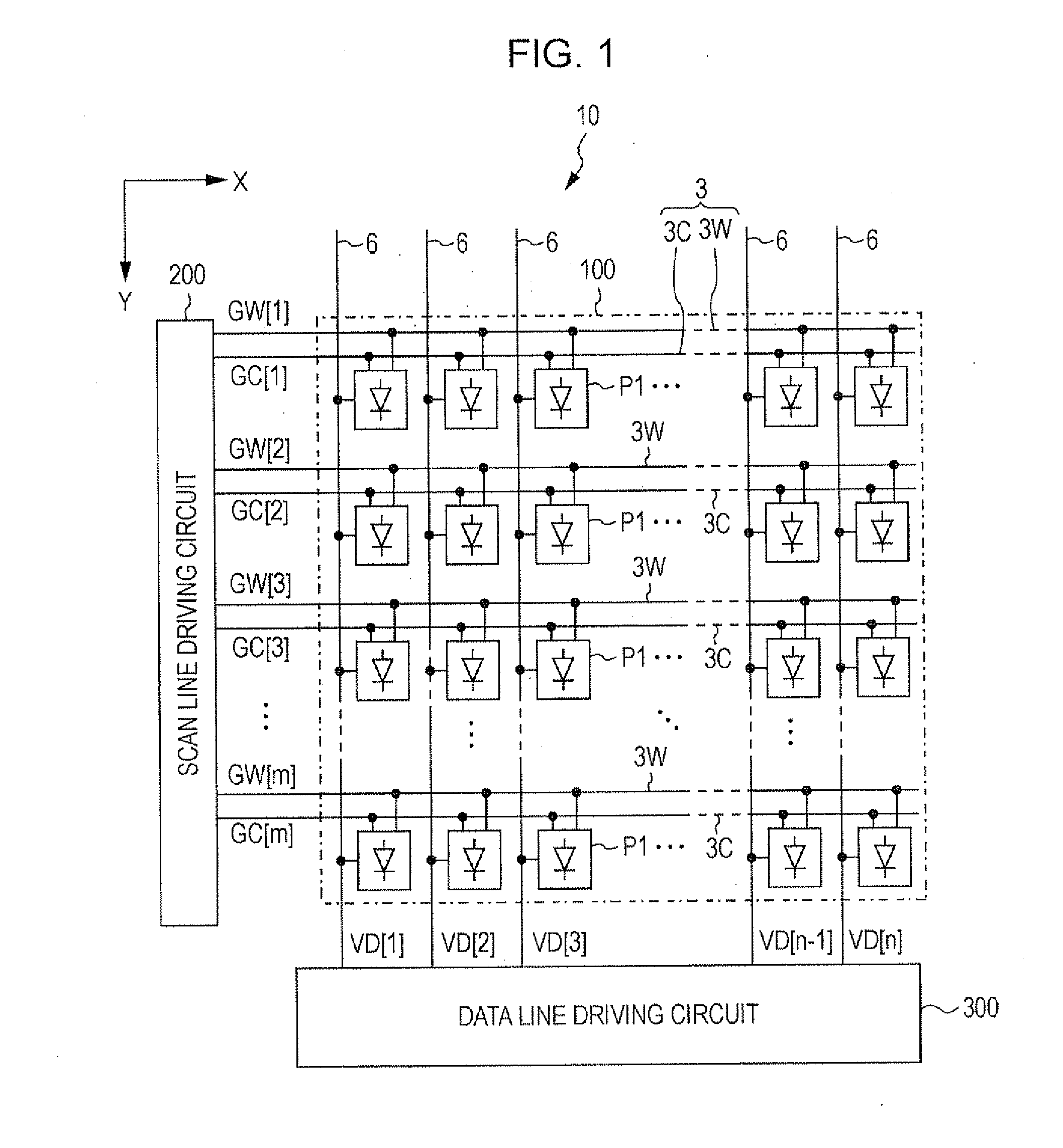
[0066]In FIG. 1, an electro-optic device 10 is a device which is adopted in various types of electronic devices as a device for displaying an image, and includes a pixel array section 100 in which a plurality of unit circuits P1 is arranged in a planar shape; a scan line driving circuit 200 and a data line driving circuit 300. In the meantime, although the scan line driving circuit 200 and the data line driving circuit 300 are shown as a separate circuit in FIG. 1, the configuration where all or a portion of these circuits are composed of a single circuit may be also adopted.

[0067]As shown in FIG. 1, the pixel array section 100 is provided with m scan lines 3 extending in an X direc...

second embodiment

[0110]Hereinafter, a second embodiment according to the invention will be described with reference to FIG. 10 to FIG. 13. Meanwhile, the second embodiment is characterized in that a configuration of a unit circuit P2 and an operation example involved undergo a modification as viewed from the first embodiment, and is similar to the configuration and the operation or the action of the first embodiment with respect to other points. Therefore, hereinafter, the difference is mainly described, and a description of other differences is properly simplified, or is omitted.

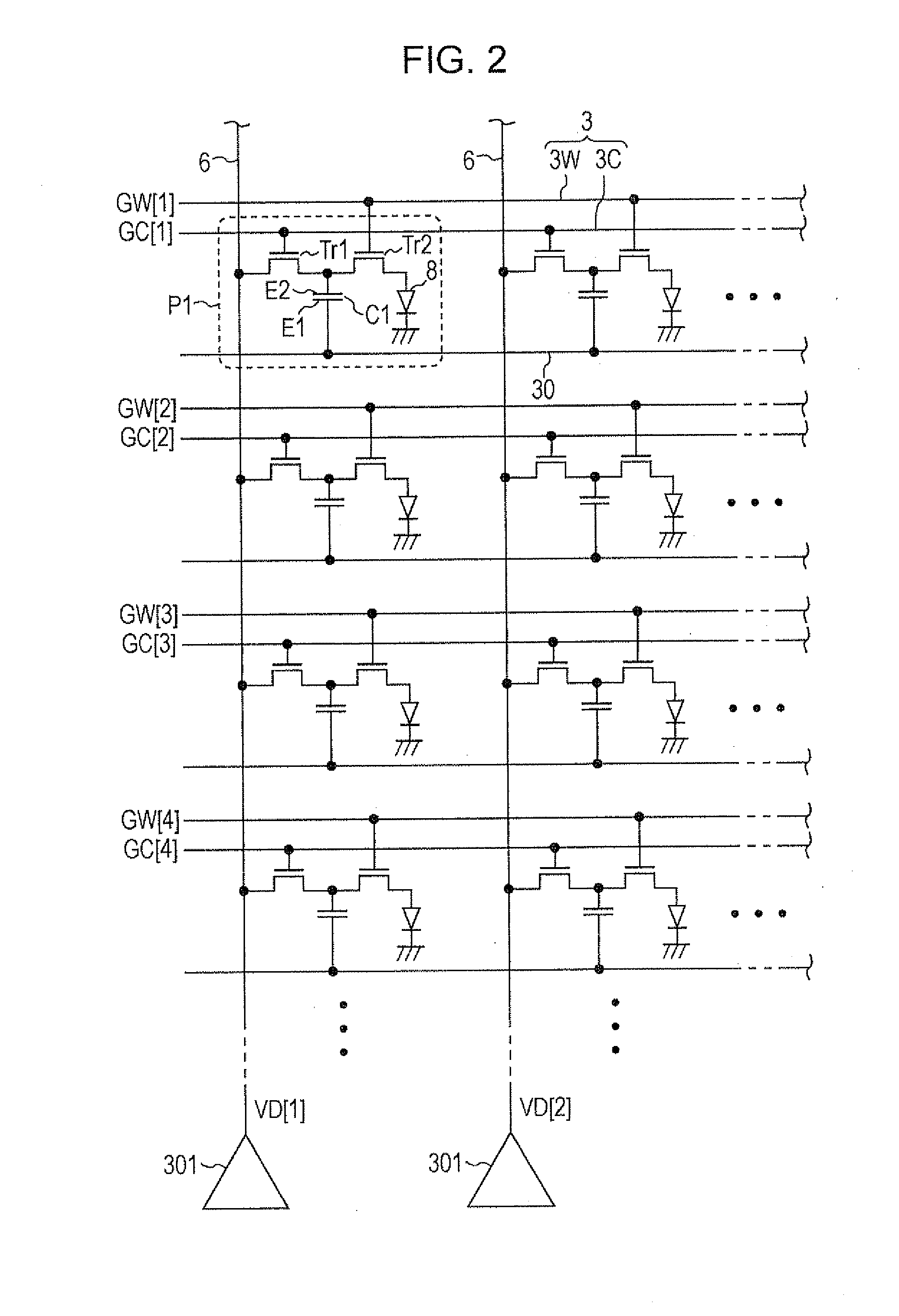
[0111]In the second embodiment, as shown in FIG. 10, the configuration of the unit circuit P2 is different from the configuration of the unit circuit P1 according to the first embodiment. That is, in the unit circuit P2, the drain of the first transistor Tr1 is connected to a node N1 on the data line 6, and the source thereof is connected to the second electrode 52 of the capacitor element C1. On the other hand, in this uni...


PUM


Abstract

An electro-optic device is provides, which includes: a plurality of unit circuits disposed corresponding to intersection of a plurality of scan lines and a plurality of data lines; control lines extended corresponding to the plurality of each of the scan lines; a scan line driving circuit that sequentially selects one of the scan lines for each drive period within each unit period, and selects all or a portion of the plurality of control lines; and a data line driving circuit that outputs a data potential, in response to grayscale data of the unit circuit corresponding to the scan line selected in the drive period within the unit period, to each of the data lines, for each period within the unit period which is a writing period before the drive period is started.

Description

BACKGROUND[0001]1. Technical Field[0002]The present invention relates to an electro-optic device including an organic EL (electroluminescent) element, a liquid crystal and the like, a driving method thereof and an electronic device.[0003]2. Related Art[0004]Hitherto, the electro-optic devices including an organic EL element and the like have been provided as electro-optic elements. In this electro-optic device, various driver circuits are included in order to supply predetermined current or voltage for the organic EL element and the like. Such driver circuit may include, for example, a capacitor element that is connected in parallel in addition to the organic EL element. In such a case, the data potential is supplied to the positive electrode of the organic EL element and one electrode of the capacitor element, and the reference potential is supplied to the negative electrode of the organic EL element and the other electrode of the capacitor element. By this, it is possible to perfo...

Claims


Application Information

Patent Timeline
IPC IPC(8): G09G5/10H05B44/00
CPCG09G3/3258G09G2300/0842G09G2320/0626G09G2320/0228G09G2310/0248
Inventor KASAI, TOSHIYUKI
Owner SEIKO EPSON CORP
Why Eureka
Try Eureka