Semiconductor light emitting device and method for manufacturing the same

Active Publication Date: 2010-10-21
NICHIA CORP
View PDF2 Cites 38 Cited by
  • Summary
  • Abstract
  • Description
  • Claims
  • Application Information

AI Technical Summary

Benefits of technology

[0018]In the configuration described above, the semiconductor light emitting device is provided with the first convex area and the second convex area in the light extraction surface, and the second convex area is disposed adjacent to the electrode. Therefore, a peeling-off of the electrode of the light emitting device can be reduced in comparison with that of a light emitting device which is uniformly provided with only the first convex which is formed from a relatively deep level on the light extraction surface, while homogenizing a current dispersion in the semiconductor layer. In addition, a light distribution of the semiconductor light emitting device can be improved in comparison with that of a semiconductor light emitting device which is uniformly provided with only the first convex which is formed from a relatively deep level in the light extraction surface, as well as provided with no concaves / convexes in an area adjacent to the electrode. Furthermore, a light output of the semiconductor light emitting device can be increased in comparison with that of a semiconductor light emitting device which is uniformly provided with only the second convex which is formed from a relatively shallow level in the light extraction surface.
[0031]According to the semiconductor light emitting device of the present invention, a peeling-off of the electrode on the side of the light extraction surface can be reduced, and a current dispersion in the semiconductor layer can be homogenized, while increasing the light extraction efficiency. Then, a semiconductor light emitting device which is highly reliable and excellent in light output can be provided. In addition, the light output has a maximum value at directivity angle 0°, and the light distribution is close to the Lambert's law. Therefore, a semiconductor light emitting device suitable for, for example, lighting can be provided. In addition, according to the present invention, a semiconductor light emitting device which is highly reliable and excellent in light distribution can be fabricated, while shortening the fabrication process. Here, the excellent light distribution in the present invention means that the light output has the maximum value at directivity angle 0°, and the light distribution is close to the Lambert's law. As a result, a light emitting device which is excellent and easy in designing of, for example, lighting or an automobile headlamp can be obtained.

Problems solved by technology

However, there were the following problems in the conventional technologies.
Therefore, in the case that improves a light output as well as the light extraction efficiency, the following problems will be caused.
For example, the light emitting device described in JPn. Pat. Appln. KOKAI Publication No. 2000-196152 is poor in the light distribution because concaves / convexes formed on a semiconductor layer surface are formed in semispherical.
That is, a light extraction efficiency of a light emitted outside from the concaves / convexes in the right upper direction becomes poor.

Method used


Image

  • Semiconductor light emitting device and method for manufacturing the same
  • Semiconductor light emitting device and method for manufacturing the same
  • Semiconductor light emitting device and method for manufacturing the same

Examples


Embodiment Construction

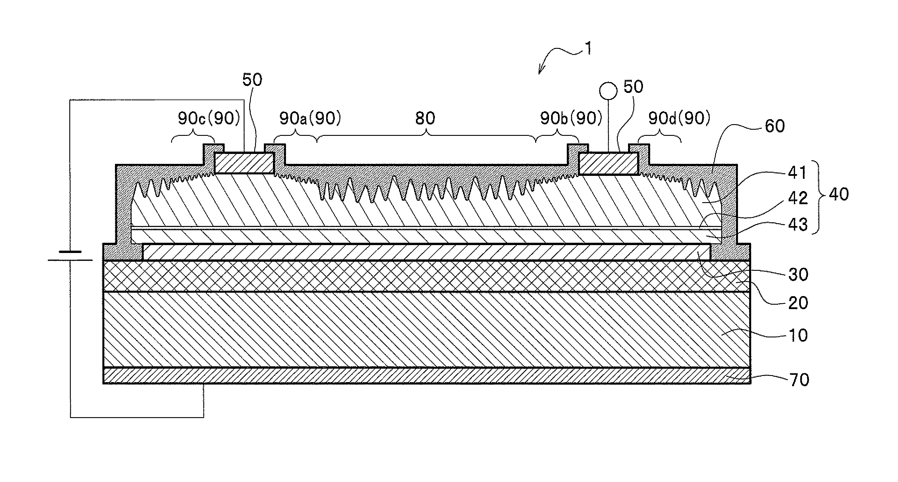
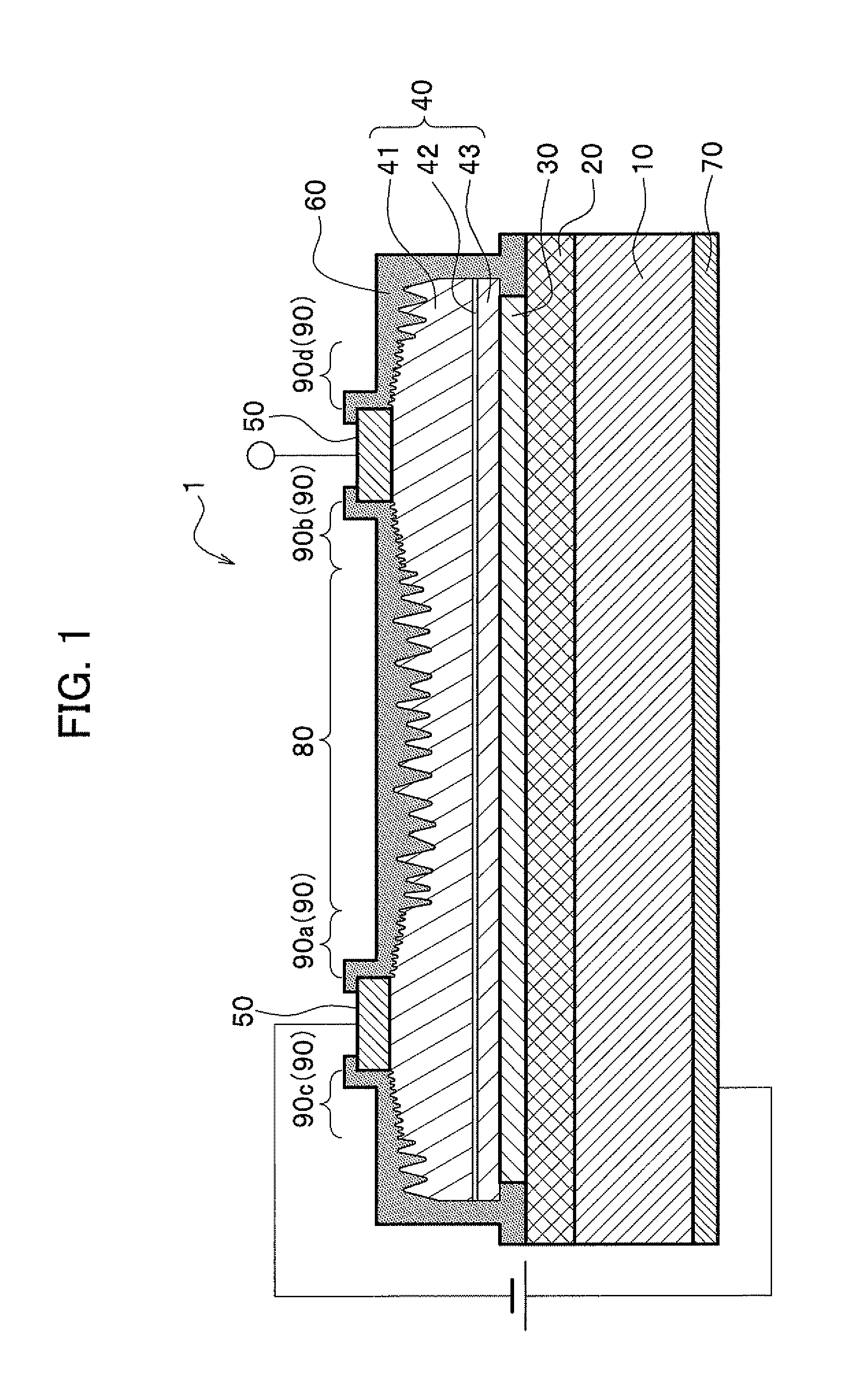
[0045]Hereinafter, a best mode (hereinafter, referred to as embodiment) for embodying a semiconductor light emitting device according to the present invention will be explained by referring to drawings. It is noted that thicknesses and lengths of, for example, constituents shown in the drawings are enlarged for the purpose of clearly explaining the arrangements, then, the thicknesses and lengths are not limited to those shown in the drawings.

[Structure of Light Emitting Device]

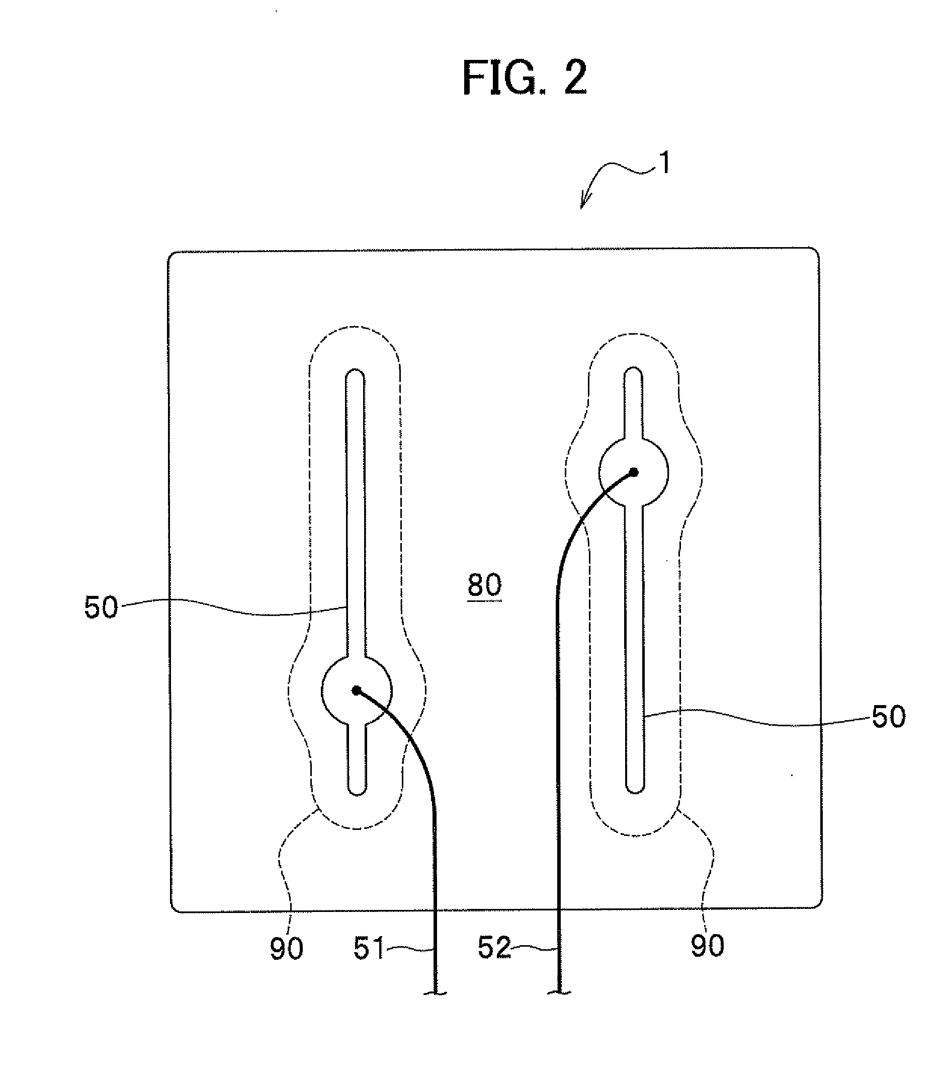
[0046]A light emitting device according to an embodiment of the present invention relates to a light emitting device which is provided with a plurality of convexes and an electrode on a light extraction surface of a semiconductor stack, which has a light emitting layer between an n-type semiconductor layer and a p-type semiconductor layer, opposite to the surface to be mounted on a substrate. First, a structure of the semiconductor light emitting device will be explained by referring to FIG. 1 to FIG. 4. FIG. ...


PUM


Abstract

A semiconductor light emitting device having high reliability and excellent light distribution characteristics is provided. Specifically, a semiconductor light emitting device 1 is provided with an n-electrode 50, which is arranged on a light extraction surface on the side opposite to the surface whereupon a semiconductor stack 40 is mounted on a substrate 10. A plurality of convexes are arranged on a first convex region 80 and a second convex region 90 on the light extraction surface. The second convex region 90 adjoins to the interface between the n-electrode 50 and the semiconductor stack 40, between the first convex region 80 and the n-electrode 50. The base end of the first convex arranged in the first convex region 80 is positioned closer to alight emitting layer 42 than the interface between the n-electrode 50 and the semiconductor stack 40, and the base end of the second convex arranged in the second convex region 90 is positioned closer to the interface between the n-electrode 50 and the semiconductor stack 40 than the base end of the first convex.

Description

FIELD OF THE INVENTION[0001]The present invention relates to a semiconductor light emitting device, and more particularly relates to a semiconductor light emitting device which is provided with concaves / convexes on a light extraction surface for increasing light extraction efficiency, and a fabrication method for the same.DESCRIPTION OF THE RELATED ART[0002]Conventionally, in the light emitting device such as LED, a plurality of concaves / convexes may be formed on a semiconductor layer surface of the light extraction side for increasing light extraction efficiency from the semiconductor layer, and the electrode is also formed on a part of the semiconductor layer surface. Such technologies described in, for example, JPn. Pat. Appln. KOKAI Publication No. 2000-196152, JPn. Pat. Appln. KOKAI Publication No. 2005-5679, JPn. Pat. Appln. KOKAI Publication No. 2003-69075, JPn. Pat. Appln. KOKAI Publication No. 2005-244201 and JPn. Pat. Appln. KOKAI Publication No. 2006-147787 have been know...

Claims


Application Information

Patent Timeline
IPC IPC(8): H01L33/02H01L33/20H01L33/22H01L33/36H01L33/44
CPCH01L33/20H01L33/22H01L33/36H01L33/44H01L2933/0058H01L33/0079H01L33/005H01L2933/0016H01L33/007H01L33/382H01L33/0093
Inventor WAKAI, YOHEIMATSUMURA, HIROAKIOKA, KENJI
Owner NICHIA CORP
Why Eureka
Try Eureka