Liquid crystal display device having black matrix in region outside of pixel region and method for fabricating the same

Active Publication Date: 2005-12-29
LG DISPLAY CO LTD
View PDF16 Cites 8 Cited by
  • Summary
  • Abstract
  • Description
  • Claims
  • Application Information

AI Technical Summary

Benefits of technology

[0021] An object of the present invention is to provide a liquid crystal display device having a black matrix in an outside region, thereby preventing light leakage occurring at the outside region. The black matrix in the outside region is extended from a pixel region or is an black matrix in addition to a black matrix in the pixel region.
[0023] Yet, another object of the present invention is to provide a method for fabricating a liquid crystal display device having shortened fabricating process by forming a black matrix in an outside region when forming a black matrix in a pixel region on an array substrate.

Problems solved by technology

However, the LCD device in which the black matrix is formed on the color filter substrate is disadvantageous in that it is difficult to precisely attach the array substrate and color filter substrate together.
Thus, an additional black matrix 173 of an opaque metal layer is formed on the upper substrate 150 corresponding to the outside region O. As a result, a black matrix forming process is performed twice, one in an array substrate fabricating process and another in an upper substrate fabricating process, thereby reducing production efficiency and increasing fabrication costs.

Method used


Image

  • Liquid crystal display device having black matrix in region outside of pixel region and method for fabricating the same
  • Liquid crystal display device having black matrix in region outside of pixel region and method for fabricating the same
  • Liquid crystal display device having black matrix in region outside of pixel region and method for fabricating the same

Examples


Embodiment Construction

[0035] Reference will now be made in detail to the preferred embodiments of the present invention, examples of which are illustrated in the accompanying drawings.

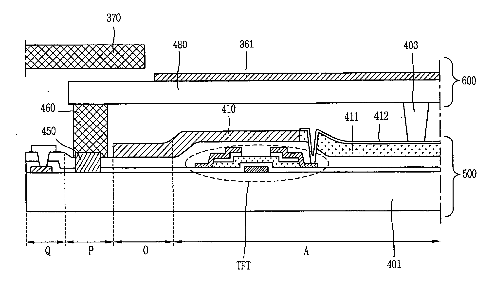
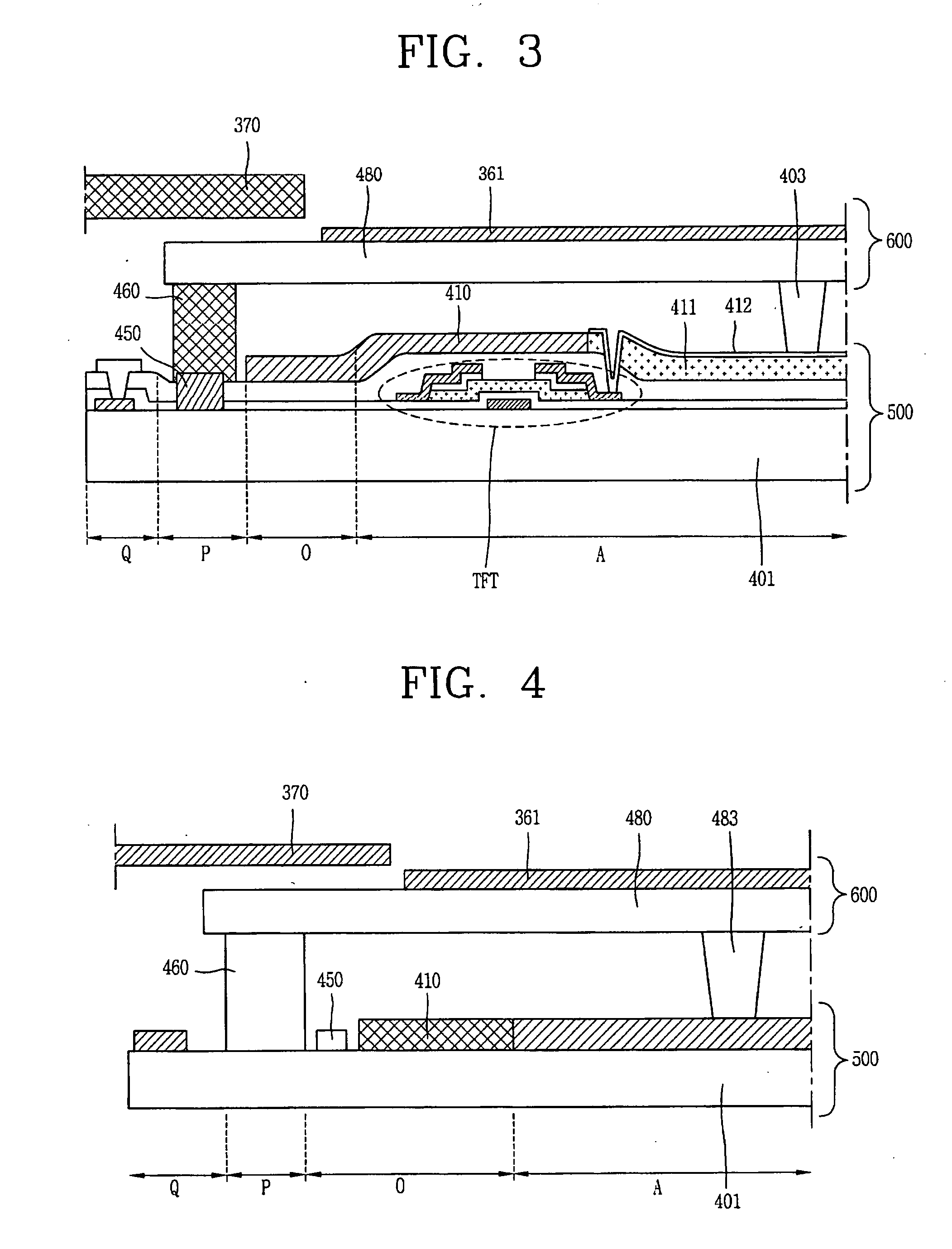
[0036]FIG. 3 is a cross-sectional view illustrating a COT type LCD device in accordance with an embodiment of the present invention. In FIG. 3, an LCD device includes an array substrate 500 including a color filter layer and an upper substrate 600 facing the array substrate 500. The array substrate 500 and the upper substrate 600 are attached together by a seal pattern 460. A plurality of gate lines (not shown) and a plurality of data lines (not shown) intersecting the gate lines are formed in a pixel region A on a lower substrate 401 of the array substrate 500, thereby defining a plurality of unit pixels.

[0037] In addition, a thin film transistor (TFT), which is a switching device, is formed at one side of each of the unit pixels on the array substrate 500. The TFT applying data voltage to the unit pixel is insulated fro...


PUM


Abstract

A color filter on thin film transistor (COT) type liquid crystal display device includes a pixel region having a plurality of unit pixels defined by intersections of gate and data lines, the gate and data lines formed on a first substrate, a pad region receiving driving signals and applying the driving signals to the gate and data lines, a seal pattern between the pad region and the pixel region, an outside region having a first black matrix, the outside region being between the seal pattern and the pixel region and the first black matrix formed on the first substrate, and an electrostatic discharge circuit between the pad region and the pixel region, the electrostatic discharge circuit formed on the first substrate.

Description

[0001] The present invention claims the benefit of Korean Patent Application No. 49779 / 2004 filed in Korea on Jun. 29, 2004, which is hereby incorporated by reference. BACKGROUND OF THE INVENTION [0002] 1. Field of the Invention [0003] The present invention relates to a liquid crystal display device, and more particularly, to a color filter on thin film transistor type liquid crystal display device having a black matrix in an outside region immediately adjacent to a pixel region. [0004] 2. Discussion of the Related Art [0005] A liquid crystal display (LCD) device is a display device for displaying an image using liquid crystal molecules having a refractive anisotropy and a dielectric anisotropy. In general, an LCD device includes an array substrate in which unit pixels are arranged in a matrix form, a color filter substrate facing the array substrate and displaying an image in color, and a liquid crystal layer between the array substrate and the color filter substrate. [0006] A TN (...

Claims


Application Information

Patent Timeline
IPC IPC(8): G02F1/1335G02F1/1362
CPCG02F2001/136222G02F1/136204G02F1/136222G02F1/1335
Inventor KIM, DONG-GUK
Owner LG DISPLAY CO LTD
Why Eureka
Try Eureka