
Semiconductor Chip Package with Stiffener Frame and Configured Lid

a technology of semiconductor chip and stiffener frame, which is applied in the direction of semiconductor/solid-state device details, electrical apparatus, semiconductor devices, etc., can solve the problems of reducing electrical pathways without inducing potentially damaging substrate warping, and the tendency of conventional substrates to still warp

Active Publication Date: 2010-11-04
ADVANCED MICRO DEVICES INC
View PDF31 Cites 66 Cited by
  • Summary
  • Abstract
  • Description
  • Claims
  • Application Information

AI Technical Summary

Problems solved by technology

Even with that provided stiffness, conventional substrates still tend to warp due to mismatches in coefficients of thermal expansion for the chip, underfill and substrate.
The difficult problem is how to reduce the electrical pathways without inducing potentially damaging substrate warping.
Even after curing, particles of the glue may sprinkle down on sensitive electronic structures, such as tiny socket structures, and cause electrical problems.

Method used


Image

  • Semiconductor Chip Package with Stiffener Frame and Configured Lid
  • Semiconductor Chip Package with Stiffener Frame and Configured Lid
  • Semiconductor Chip Package with Stiffener Frame and Configured Lid

Examples


Embodiment Construction

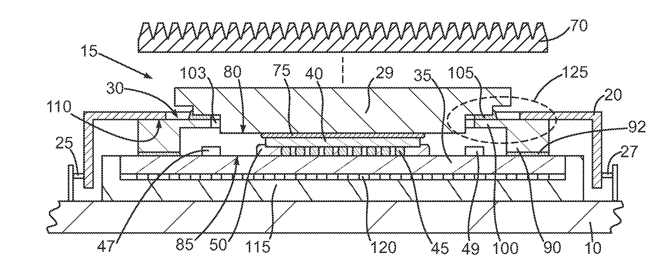
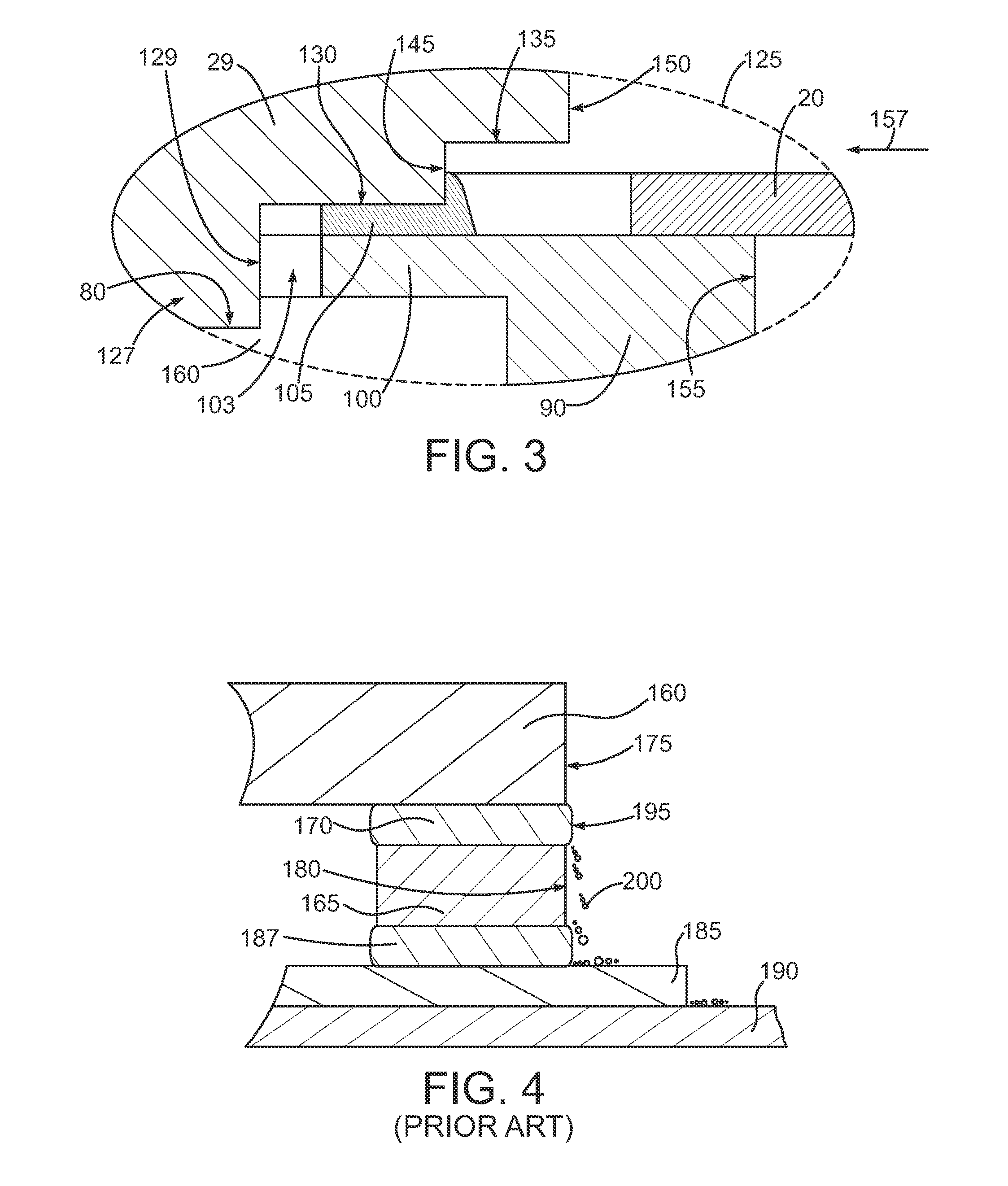
[0023]Various embodiments of a semiconductor chip package with a stiffener frame and a configured lid are described herein. One example includes a stiffener frame that has a laterally inwardly projecting extension that provides a seating surface for an adhesive. The lid is configured with a first flange that seats on the frame extension and provides a surface that readily attracts the adhesive at a setback distance from the edge of the stiffener frame. Additional details will now be described.

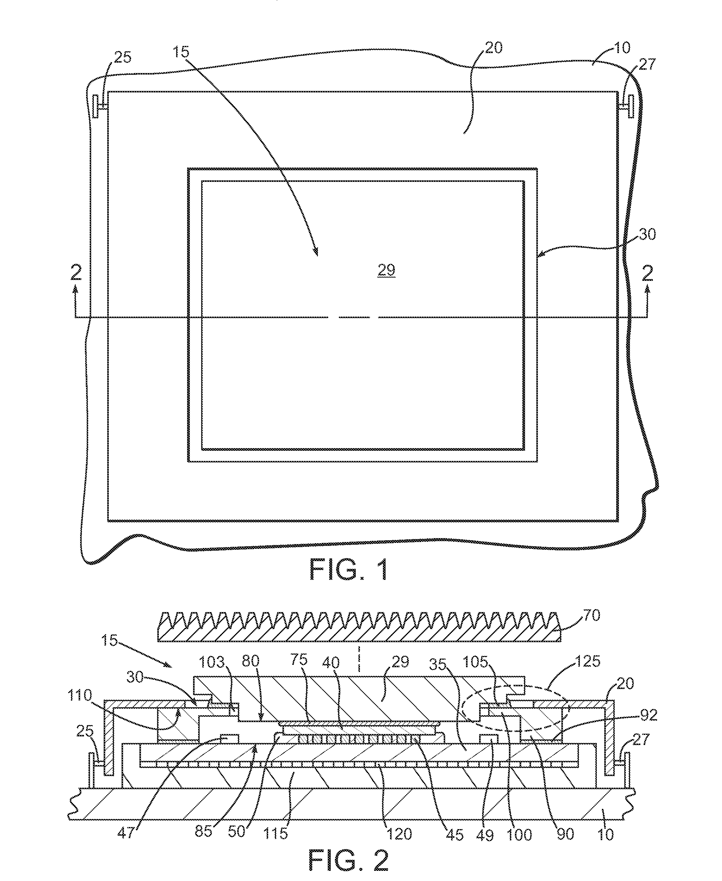
[0024]In the drawings described below, reference numerals are generally repeated where identical elements appear in more than one figure. Turning now to the drawings, and in particular to FIG. 1, therein is shown FIG. 1 which is an overhead view of a small portion of a printed circuit board 10 and a semiconductor chip package 15 secured to the printed circuit board 10 by way of a clamp 20. The printed circuit board 10 may be virtually any type of circuit board. Examples include motherboards, ci...


PUM


Abstract

Various semiconductor chip packages and methods of assembling and making the same are disclosed. In one aspect, a method of manufacturing is provided that includes coupling a stiffener frame to a first side of a substrate. The stiffener frame has a central opening to accommodate a semiconductor chip and an outer edge surface. A semiconductor chip is coupled to the first side in the opening. A lid is coupled to the stiffener frame with an adhesive. The lid has a first edge surface set back from the outer edge surface of the stiffener frame. The adhesive is set back from the outer edge surface of the stiffener frame.

Description

BACKGROUND OF THE INVENTION[0001]1. Field of the Invention[0002]This invention relates generally to semiconductor processing, and more particularly to semiconductor chip packages utilizing stiffener frames and methods of making the same.[0003]2. Description of the Related Art[0004]Many current integrated circuits are formed as multiple dice on a common silicon wafer. After the basic process steps to form the circuits on the dice are complete, the individual dice are cut or singulated from the wafer. The singulated dice are then usually mounted to structures, such as circuit boards, or packaged in some form of enclosure. One frequently-used package consists of a substrate upon which a die is mounted. The upper surface of the substrate includes electrical interconnects. The die is manufactured with a plurality of bond pads. A collection of solder bumps are provided between the bond pads of the die and substrate interconnects to establish ohmic contact. An underfill material is deposit...

Claims


Application Information

Patent Timeline
IPC IPC(8): H01L23/04H01L21/50
CPCH01L21/50H01L23/10H01L23/16H01L23/36H01L23/42H01L2224/16H01L2924/19105H01L2924/16152H01L2224/16225H01L2224/32245H01L2224/73253H01L2924/1531H01L2924/01078H01L2924/00014H01L2924/00011H01L2224/0401
Inventor HENG, STEPHEN F.DANDIA, SANJAYLEONG, CHIA-KEN
Owner ADVANCED MICRO DEVICES INC
Features
  • Generate Ideas
  • Intellectual Property
  • Life Sciences
  • Materials
  • Tech Scout
  • Unparalleled Data Quality
  • Higher Quality Content
  • 60% Fewer Hallucinations
Learn More