Method of testing for a leakage current between bit lines of nonvolatile memory device
- Summary
- Abstract
- Description
- Claims
- Application Information
AI Technical Summary
Benefits of technology
Problems solved by technology
Method used
Image
Examples
Embodiment Construction
[0020]Hereinafter, embodiments of the present invention are described in detail with reference to the accompanying drawings. The drawing figures are provided to allow those having ordinary skill in the art to understand the scope of the embodiments of the present invention.
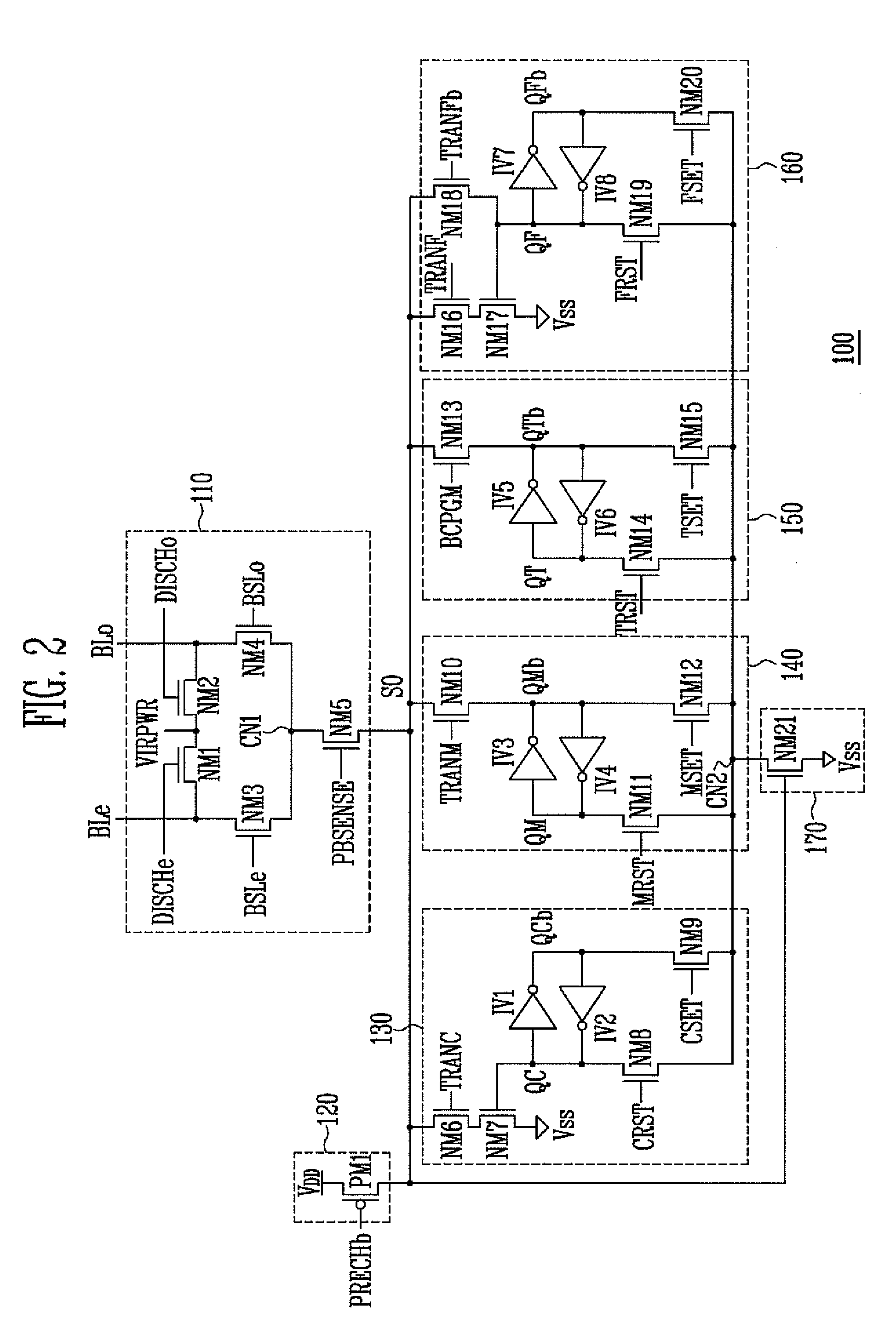
[0021]FIG. 2 is a circuit diagram of a page buffer for illustrating a method of testing for a leakage current between the bit lines of a nonvolatile memory device according to an embodiment of the present invention.
[0022]Referring to FIG. 2, the page buffer 100 includes a bit line selection unit 110, a precharge unit 120, a cache latch 130, a main latch 140, a temporary latch 150, a flag latch 160, and a sense unit 170.
[0023]The bit line selection unit 110 includes a number of NMOS transistors NM1 to NM5. The NMOS transistor NM1 and the NMOS transistor NM2 are coupled in series between an even bit line BLe and an odd bit line BLo, coupled to a memory cell array, and are configured to supply a test voltage VIRPWR t...
PUM
 Abstract
Description
Claims
Application Information


