
Circuit and technique for accurately sensing low voltage flash memory devices

Active Publication Date: 2005-11-08
MONTEREY RES LLC
View PDF5 Cites 8 Cited by
  • Summary
  • Abstract
  • Description
  • Claims
  • Application Information

AI Technical Summary

Benefits of technology

[0005]The present invention addresses and resolves the need in the art for a sensing circuit and technique for accurately sensing low voltage flash memory devices. The invention also resolves the need in the art for a sensing circuit which improves the sense margin for low voltage flash memory devices during read memory operations.
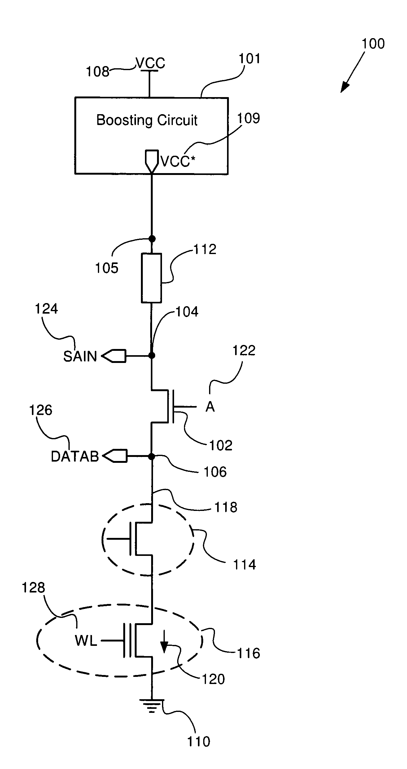
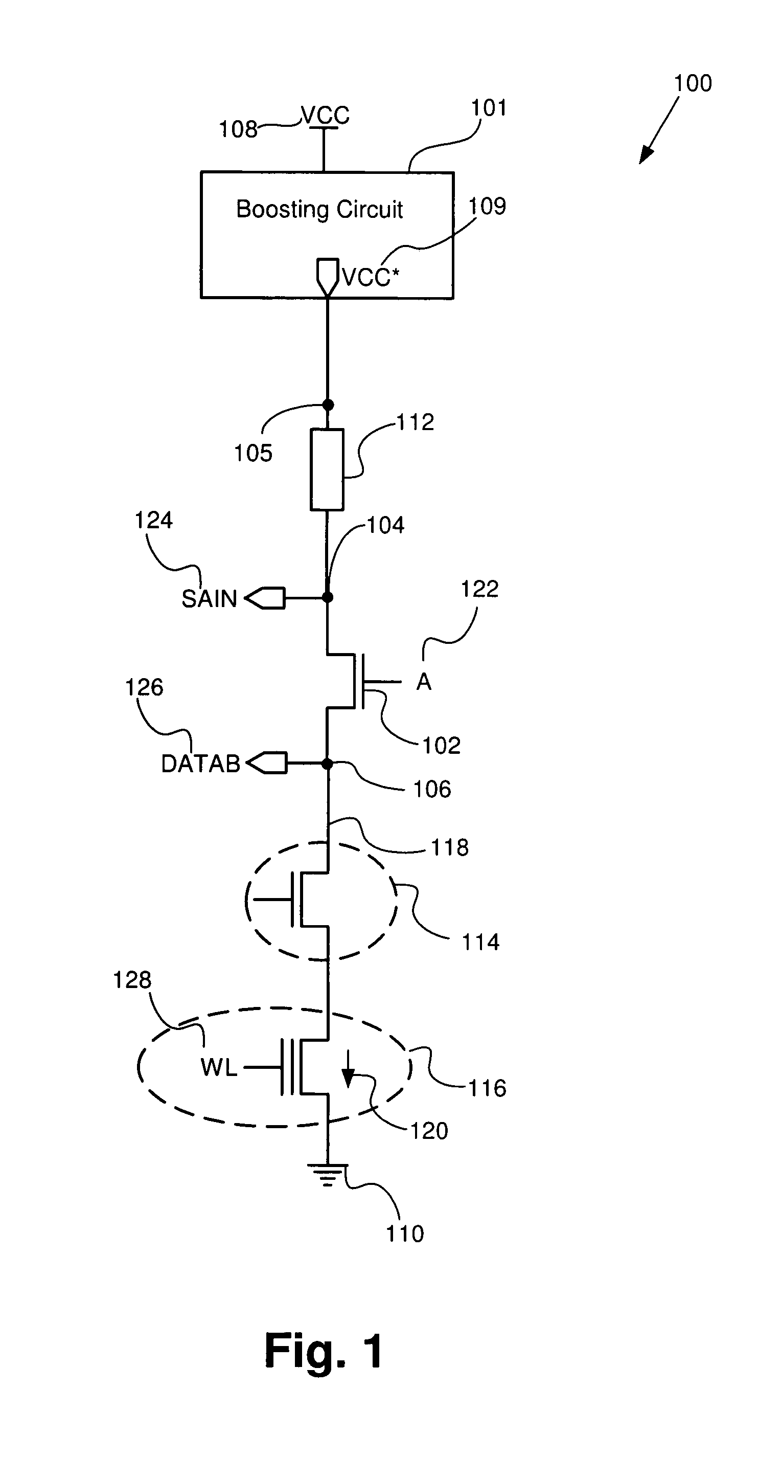
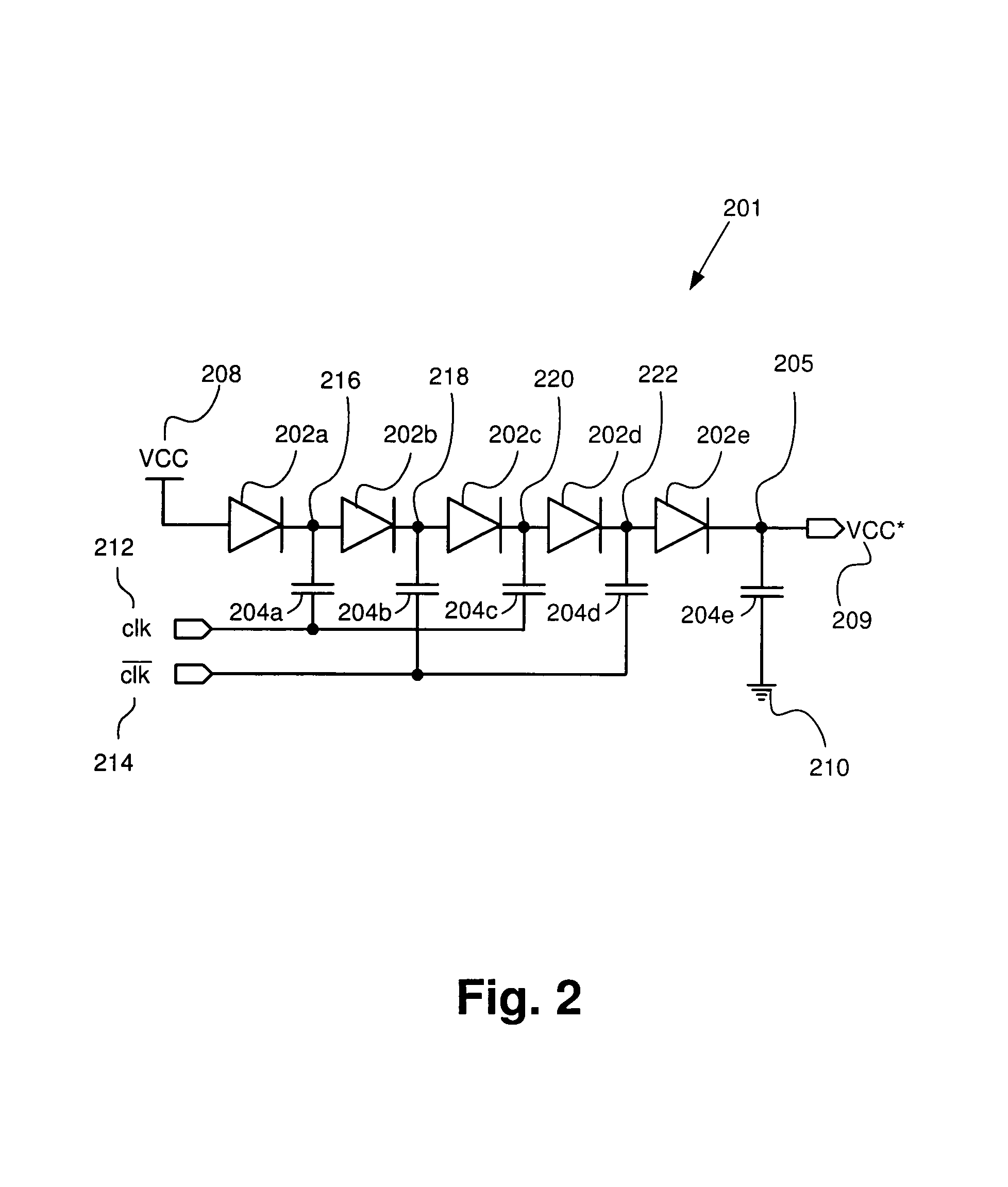
[0006]According to one exemplary embodiment, a sensing circuit for sensing the current drawn by a target memory cell comprises a first transistor connected across a first node and a second node, a load connected across the second node and a third node, and a voltage boosting circuit coupled to a supply voltage. For example, the voltage boosting circuit can be a charge pump driven by a two-phase clock. The voltage boosting circuit supplies a voltage at the third node which is greater than the supply voltage. The target memory cell has a drain capable of being connected to the first node through a selection circuit during a read operation involving the target memory cell. During the read operation, the target memory cell draws a target memory cell current when activated, and a sense amp input voltage is generated at the second node. Due to the particular arrangement of the sensing circuit, the sense margin for sensing target memory cell current is significantly increased, and the accuracy of the memory device is significantly improved.

Problems solved by technology

The reliability and accuracy of the read operation are thus reduced, resulting in poor performance of the memory device.

Method used


Image

  • Circuit and technique for accurately sensing low voltage flash memory devices
  • Circuit and technique for accurately sensing low voltage flash memory devices
  • Circuit and technique for accurately sensing low voltage flash memory devices

Examples


Embodiment Construction

[0013]The present invention is directed to a sensing circuit and technique for accurately sensing low voltage flash memory devices. The following description contains specific information pertaining to the implementation of the present invention. One skilled in the art will recognize that the present invention may be implemented in a manner different from that specifically discussed in the present application. Moreover, some of the specific details of the invention are not discussed in order not to obscure the invention.

[0014]The drawings in the present application and their accompanying detailed description are directed to merely exemplary embodiments of the invention. To maintain brevity, other embodiments of the present invention are not specifically described in the present application and are not specifically illustrated by the present drawings.

[0015]Referring first to FIG. 1, there is shown a circuit diagram of exemplary sensing circuit 100 according to one embodiment of the p...


PUM


Abstract

An exemplary sensing circuit for sensing the current drawn by a target memory cell comprises a first transistor connected across a first node and a second node, a load connected across the second node and a third node, and a voltage boosting circuit coupled to a supply voltage, wherein the voltage boosting circuit supplies a voltage at the third node which is greater than the supply voltage.

Description

TECHNICAL FIELD[0001]The present invention relates generally to the field of semiconductor devices. More particularly, the present invention relates to semiconductor memory devices.BACKGROUND ART[0002]Memory devices are known in the art for storing data in a wide variety of electronic devices and applications. A typical memory device comprises a number of memory cells. Often, memory cells are arranged in an array format, where a row of memory cells corresponds to a word line and a column of memory cells corresponds to a bit line, and where each memory cell defines a binary bit, i.e., either a zero (“0”) bit or a one (“1”) bit.[0003]Typically, the state of a memory cell is determined during a read operation by sensing the current drawn by the memory cell. According to one particular embodiment, the current drawn by a particular memory cell is ascertained by connecting the drain terminal of the memory cell to a sensing circuit, where the source terminal of the memory cell is connected...

Claims


Application Information

Patent Timeline
IPC IPC(8): G11C16/06G11C16/26G11C16/30
CPCG11C16/26G11C16/30
Inventor WANG, ZHIGANGYANG, NIANHE, YUE-SONG
Owner MONTEREY RES LLC
Learn More