Method of driving plasma display panel, and plasma display apparatus

Inactive Publication Date: 2010-12-23
PANASONIC CORP
View PDF7 Cites 0 Cited by
  • Summary
  • Abstract
  • Description
  • Claims
  • Application Information

AI Technical Summary

Benefits of technology

[0036]In accordance with the present invention, it is possible to provide a novel method of driving a plasma display panel, which is capable of stably performing reset and capa

Problems solved by technology

However, in the configuration shown in FIG. 13, since the ramp of the rising ramp voltage and the ramp of the falling ramp voltage applied in the reset period are each set to have two stages, the time period required for the reset period can be reduced to some extent, but there is a limitation on further reduction of the reset period.
In addition, a circuit configuration for achieving the above configuration may be very complicated.
Furthermore, in the configu

Method used


Image

  • Method of driving plasma display panel, and plasma display apparatus
  • Method of driving plasma display panel, and plasma display apparatus
  • Method of driving plasma display panel, and plasma display apparatus

Examples


embodiment 1

[0052]

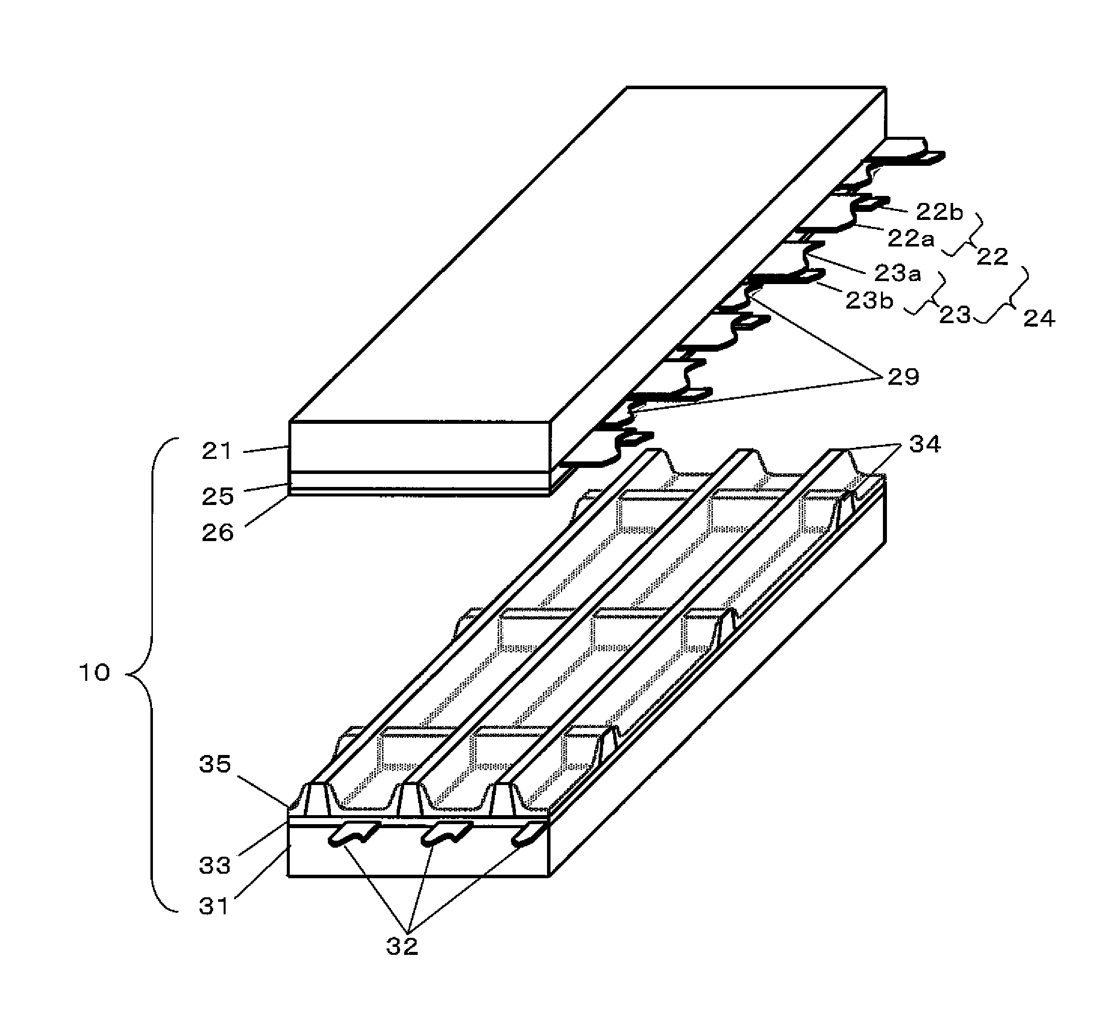
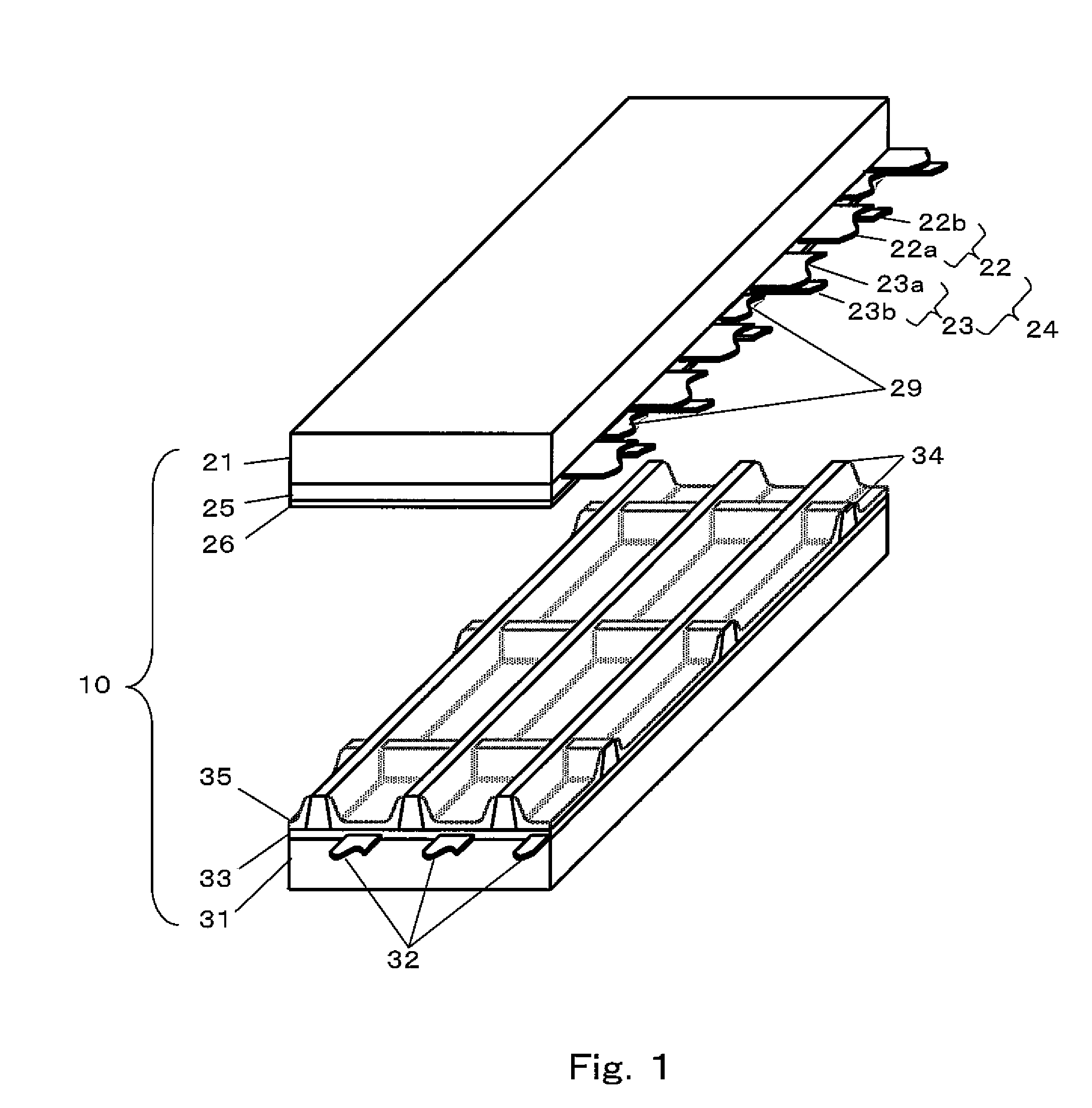
[0053]FIG. 1 is an exploded perspective view showing a structure of a plasma display panel (PDP) according to Embodiment 1 of the present invention. As shown in FIG. 1, plural display electrode pairs 24 each including a scan electrode 22 and a sustain electrode 23 are formed on a glass-made front substrate 21. Each scan electrode 22 has a transparent electrode 22a with a large width and each sustain electrode 23 has a transparent electrode 23a with a large width to generate discharge in a discharge gap between the scan electrode 22 and the sustain electrode 23 and to take out light therefrom. A bus electrode 22b with a small width is stacked on the transparent electrode 22a and a bus electrode 23b with a small width is stacked on the transparent electrode 23b such that they are respectively positioned distant from the discharge gap. A black stripe 29 is provided between adjacent display electrode pairs 24 to block light. A dielectric layer 25 and a protective layer 26 are stac...

embodiment 2

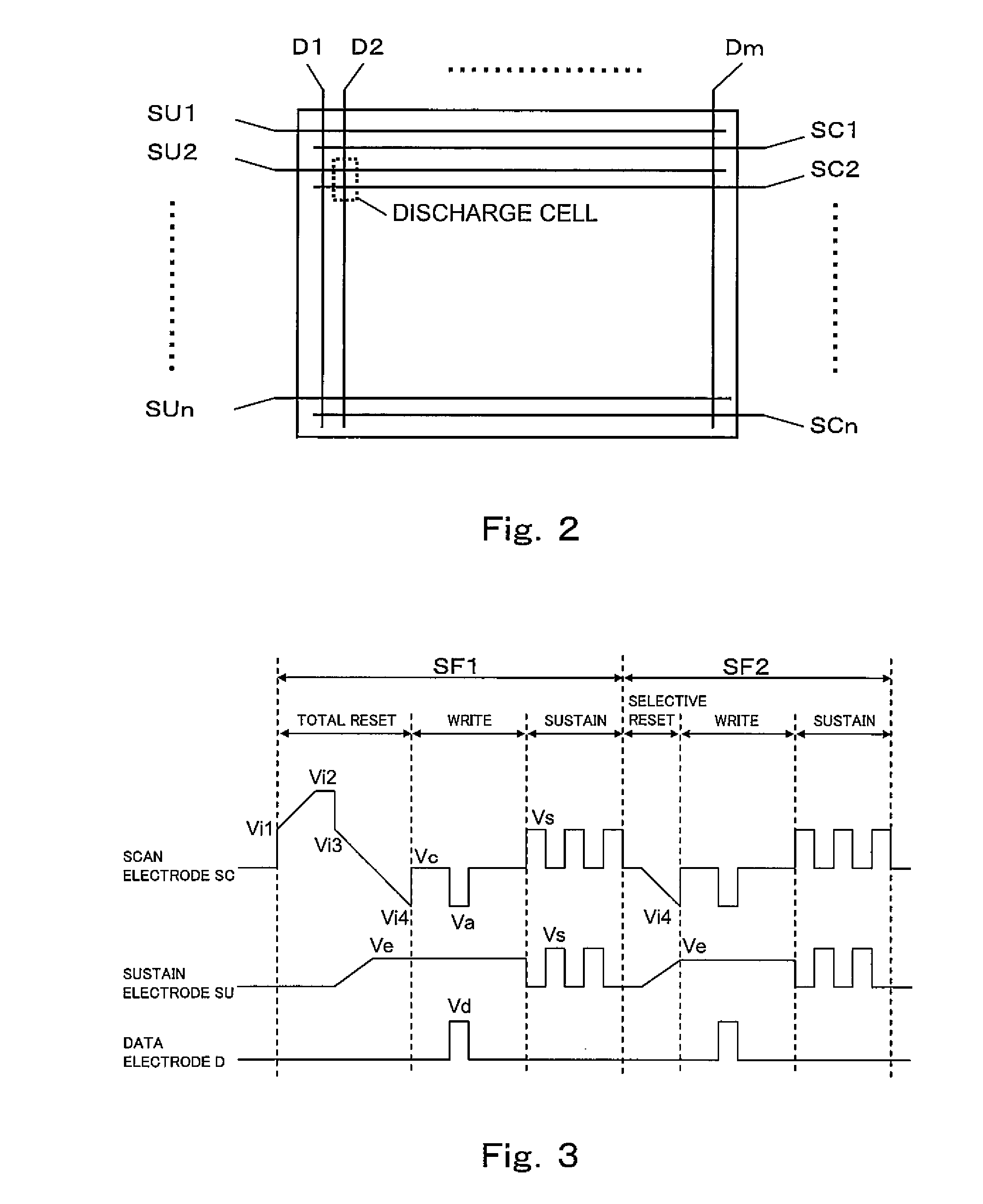
[0091]FIG. 7 is a view showing driving voltage waveforms of a driving method of a plasma display panel according to Embodiment 2 of the present invention. Embodiment 2 is different from Embodiment 1 in that in the selective reset period, the first ramp voltage and second ramp voltage are applied such that the second ramp waveform reaches a predetermined first voltage Ve and finishes rising before the first ramp waveform reaches a predetermined voltage Vi4 and finishes rising. In Embodiment 2, also, it is supposed that the panel 10 shown in FIGS. 1 and 2 is driven. Since the total reset period, the write period, and the sustain period of Embodiment 2 are similar to those of Embodiment 1, detailed description thereof will be omitted.

[0092]In Embodiment 2, as shown in FIG. 7, in the selective reset period, the first ramp voltage having a first ramp waveform gradually falling toward the voltage Vi4 which exceeds the discharge start voltage is applied to the scan electrodes SC, and a sec...

embodiment 3

[0096]FIG. 8 is a view showing driving voltage waveforms of a driving method of a plasma display panel according to Embodiment 3 of the present invention. Embodiment 3 is different from Embodiment 2 in that after the second ramp voltage reaches the first voltage Ve, the second voltage Ve2 lower than the first voltage Ve is applied to the sustain electrodes SU. In Embodiment 3, also, it is supposed that the panel 10 shown in FIGS. 1 and 2 is driven. Since the total reset period, the write period, and the sustain period of Embodiment 3 are similar to those of Embodiment 1 and Embodiment 2, detailed description thereof will be omitted.

[0097]In Embodiment 3, as shown in FIG. 8, in the selective reset period, the second ramp voltage having the second ramp waveform which is applied to the sustain electrodes SU gradually rises toward the positive first voltage Ve. After the second ramp voltage reaches the first voltage Ve, it maintains the voltage Ve for a specified period. Afterwards, the...


PUM


Abstract

A method of driving a plasma display panel of the present invention, is a driving method of a display panel including plural display electrode pairs (24) each including a scan electrode (22) and a sustain electrode (23) extending along each other, plural data electrodes (32) crossing the plural display electrode pairs (24) and discharge cells respectively formed at positions where the display electrode pairs (24) and the data electrodes (32) cross each other. The method comprises applying a last sustain pulse to the scan electrode (22) in a sustain period when a sustain voltage pulse is applied alternately to the scan electrode (22) and to the sustain electrode (23); then applying to the scan electrode (22) a first ramp voltage having a first ramp waveform which is opposite in polarity to the last sustain voltage pulse; and applying to the sustain electrode (23) a second ramp voltage having a second ramp waveform which is opposite in polarity to the first ramp voltage such that before one of the first and second ramp waveforms reaches a predetermined voltage and finishes rising, the other of the first and second ramp waveforms starts rising.

Description

RELATED APPLICATIONS[0001]This application is the U.S. National Phase under 35 U.S.C. §371 of International Application No. PCT / JP2009 / 002518, filed on Jun. 4, 2009, which in turn claims the benefit of Japanese Application Nos. 2008-147751, filed on Jun. 5, 2008 and 2009-133922, filed on Jun. 3, 2009, the disclosures of which Applications are incorporated by reference herein.TECHNICAL FIELD[0002]The present invention relates to a method of driving a plasma display panel, and a plasma display apparatus which is a display apparatus using the plasma display panel.BACKGROUND ART[0003]These days, in plasma display panels (hereinafter referred to as PDPs), AC surface discharge type PDPs are typical. In the AC surface discharge type PDP, a front substrate and a back substrate are placed so as to face each other to form a number of discharge cells. Hereinafter, the configuration of the AC surface discharge type PDP will be described.[0004]On the front substrate, plural display electrode pai...

Claims


Application Information

Patent Timeline
IPC IPC(8): G09G5/00G09G3/28G09G3/288G09G3/291G09G3/292G09G3/294G09G3/296G09G3/298
CPCG09G3/2927G09G2310/066G09G3/2965G09G3/2942
Inventor KOMINAMI, SATOSHIWAKABAYASHI, TOSHIKAZUIZUCHI, MASUMIMATSUSHITA, JUNKOARAI, YASUHIROMAKINO, HIROYASU
Owner PANASONIC CORP
Why Eureka
Try Eureka