Display device

a display device and display screen technology, applied in non-linear optics, instruments, optics, etc., to achieve the effect of further reducing the pitch between wires and reducing the frame width

Active Publication Date: 2010-12-23
PANASONIC LIQUID CRYSTAL DISPLAY CO LTD +1
View PDF5 Cites 29 Cited by
  • Summary
  • Abstract
  • Description
  • Claims
  • Application Information

AI Technical Summary

Benefits of technology

[0010]As the definition of the display devices further increases and reduction in the width of the frame and miniaturization of IC drivers further progress, the pitch between wires is further decreased. In liquid crystal display devices, wires are covered with an insulating film, for example, a passivation film, so that the wires are protected from the open air. However, it is necessary to create contact holes in this insulating film in places to which bumps of IC drivers are connected so that the wires are exposed. In addition, these contact hole portions are covered with a chemically stable transparent conductive film, such as of ITO, so that the wires do not become corroded in the contact hole portions.

Problems solved by technology

However, it is necessary to create contact holes in this insulating film in places to which bumps of IC drivers are connected so that the wires are exposed.

Method used


Image

  • Display device
  • Display device
  • Display device

Examples


first embodiment

[0088]FIGS. 18 and 19 show the first embodiment of the present invention. FIG. 18 is a plan diagram showing terminal portions, and the upper half in the figure shows a display region and the lower half shows an end of a TFT substrate 100. FIG. 19 is a cross sectional diagram along line b-b in FIG. 18.

[0089]In FIG. 18, terminal wires made of a gate metal 50 run from the display region side. The gate metal 50 has wide portions and narrow portions in the terminal portions. Contact holes 41 for a terminal are created in the wide portions of the gate metal 50. A certain width is necessary to create contact holes 41 for a terminal. Meanwhile, no contact holes 40 are created in the narrow portions of the gate metal 50 in the terminal portions. It is not necessary for the gate metal 50 to be wide, unless contact holes 40 are created.

[0090]This configuration is characterized in that one terminal 10 has a first portion 11 and a second portion 12, and a contact hole 41 for a terminal is create...

second embodiment

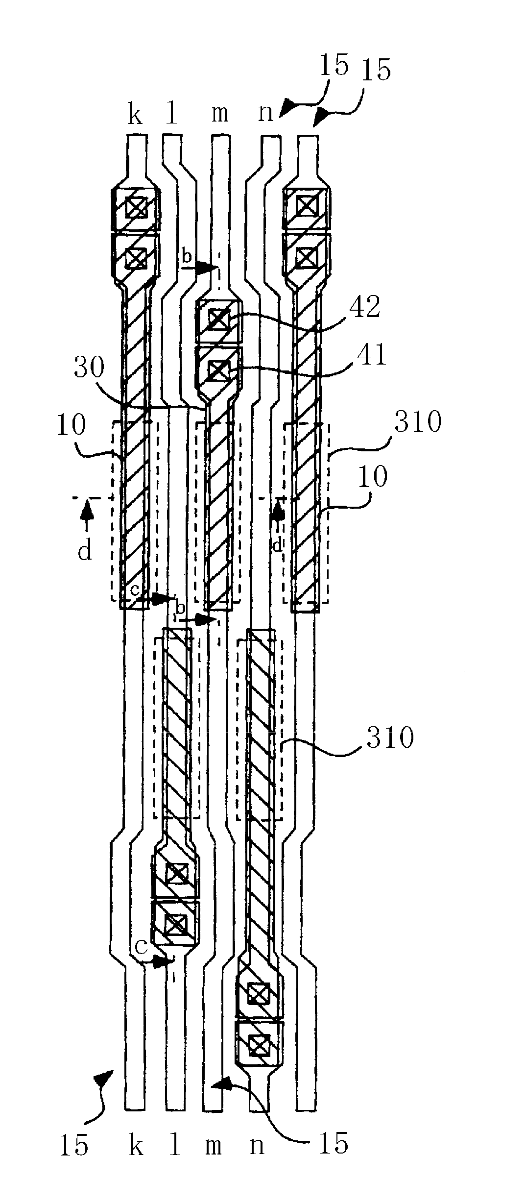
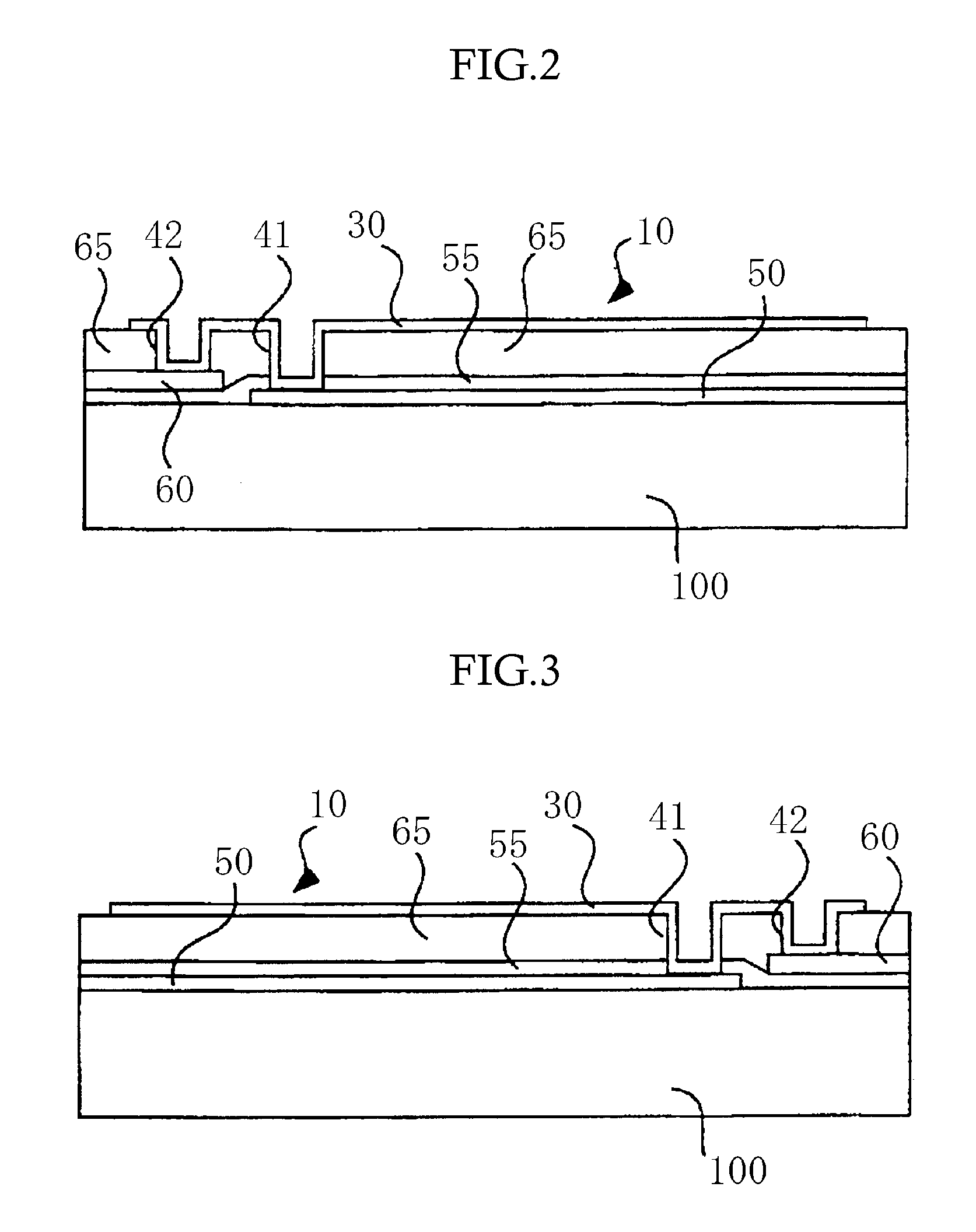
[0101]FIGS. 1 to 4 show the second embodiment of the present invention. FIG. 1 is a plan diagram showing the second embodiment. The upper half of FIG. 1 shows a display region, and the lower half of the figure shows an end of the TFT substrate 100. FIG. 2 is a cross sectional diagram along line b-b in FIG. 1, FIG. 3 is a cross sectional diagram along line c-c in FIG. 1, and FIG. 4 is a cross sectional diagram along line d-d in FIG. 1. In this, second embodiment, terminal wires 15 have a two-layer structure of a gate metal 50 and an SD metal 60. Though the present invention can also be used in cases where there is only one layer of wires in the terminal portions, as in the third embodiment, the terminal wires 15 are allowed to have a two-layer structure when the disadvantage of inaccuracy in the positioning of the mask during the photolithographic process in FIGS. 14 to 17 is unimportant.

[0102]In FIG. 1, terminal wires k and m lead out from the display region through an SD metal 60, ...

third embodiment

[0107]During the process for manufacturing a display device, there is a step of inspecting wires formed in the display device for short-circuiting at a stage before the IC driver is mounted. TFT switches, inspection wires and the like required for this inspection are formed in a region where the IC driver is to be mounted; that is to say, in the region that is hidden once the IC driver is mounted. There is a strong demand for larger display regions and smaller frames in display devices. It is preferable for the area occupied by the TFT switches, the inspection wires and the like for inspection to be as small as possible, in order to make the frame smaller.

[0108]FIGS. 5 and 6 show the configuration according to the third embodiment, where the pitch between wires in the terminal portions, as well as the area occupied by the TFT's 100 for inspection and the wires 150 for inspection, is small. FIG. 5 is a plan diagram showing the present embodiment. The upper half of FIG. 5 shows a disp...


PUM

PropertyMeasurementUnit
widthaaaaaaaaaa
widthaaaaaaaaaa
widthaaaaaaaaaa

Abstract

First terminals and second terminals, which are terminals of adjacent terminal wires, are staggered in the direction in which wires run, and transparent conductive films provided to the first terminals and second terminals extend so as to overlap the terminal wires outside the regions in which contact holes are created and are formed so as to have a width narrower than the width of the terminal wires in the regions where contact holes are created.

Description

CROSS-REFERENCE TO RELATED APPLICATION[0001]The present application claims priority over Japanese Applications JP2009-144607 filed on Jun. 17, 2009 and JP2009-144604 filed on Jun. 17, 2009, the contents of which are hereby incorporated into this application by reference.BACKGROUND OF THE INVENTION[0002](1) Field of the Invention[0003]The present invention relates to a display device, and in particular, to a technology for connecting IC drivers to wires of which the pitch has become smaller as the display devices are miniaturized, the definition of the screens increases, and the IC drivers are miniaturized.[0004](2) Description of the Related Art[0005]Liquid crystal display devices are formed such that pixel electrodes and thin film transistors (TFT's) are formed in a matrix on a TFT substrate to which a facing substrate, where color filters are formed in locations corresponding to the pixel electrodes, is attached so that liquid crystal is sandwiched between the TFT substrate and th...

Claims


Application Information

Patent Timeline
Patent Type & Authority Applications(United States)
IPC IPC(8): G02F1/1345
CPCG02F1/1345G02F1/1309G02F1/13458
Inventor YANAGISAWA, SYOU
Owner PANASONIC LIQUID CRYSTAL DISPLAY CO LTD
Why Eureka
Try Eureka