Semiconductor device having plurality of wiring layers and designing method thereof

Active Publication Date: 2010-12-30
LONGITUDE LICENSING LTD
View PDF1 Cites 26 Cited by
  • Summary
  • Abstract
  • Description
  • Claims
  • Application Information

AI Technical Summary

Benefits of technology

[0013]Thus, according to the present invention, because contact conductors connecting wiring layers that are two or more layers apart are arranged in one direction, prohibited areas that are formed in an intermediate wiring layer can be made smaller. Therefore, the flexibility of the layout of the intermediate wiring layer is enhanced and restriction on the wiring density can be relaxed.

Problems solved by technology

In order to fulfill user requirements, logic circuits formed on a semiconductor device such as DRAM (Dynamic Random Access Memory) are becoming increasingly complicated.
Consequently, it is necessary to connect to a power line of lower layers at a number of places, so that contact conductors used for this purpose restrict the layout of the intermediate wiring layers.

Method used


Image

  • Semiconductor device having plurality of wiring layers and designing method thereof
  • Semiconductor device having plurality of wiring layers and designing method thereof
  • Semiconductor device having plurality of wiring layers and designing method thereof

Examples


first embodiment

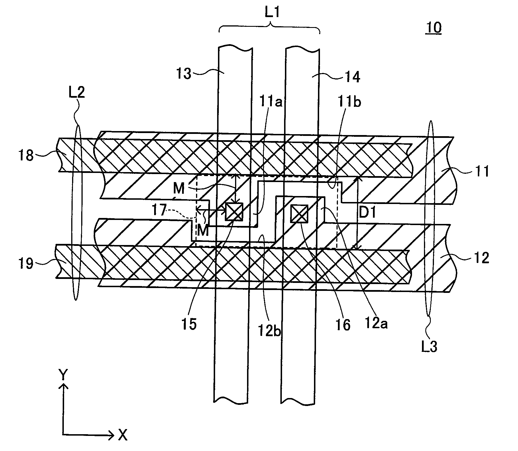
[0024]FIG. 1 is a schematic plan view of a wiring layout of a semiconductor device 10 according to the present invention.

[0025]The semiconductor device 10 shown in FIG. 1 has at least three wiring layers, the relatively upper wiring layer L3 has wirings 11 and 12 extending parallel to an X direction, and the relatively lower wiring layer L1 has wirings 13 and 14 extending parallel to a Y direction. The wirings 11 and 13 are supplied with the same signal or the same electric potential and they are connected to each other with a contact conductor 15. Similarly, the wirings 12 and 14 are supplied with the same signal or the same electric potential and they are connected to each other with a contact conductor 16. The wirings 11 and 13 are power lines supplied with a predetermined electric potential (for example, VDD) and the wirings 12 and are power lines supplied with an electric potential different from the above electric potential (for example, VSS). However, the configuration is not...

second embodiment

[0031]FIG. 3 is a schematic plan view of a wiring layout of a semiconductor device 20 according to the present invention.

[0032]The semiconductor device 20 shown in FIG. 3 is different from the semiconductor device 10 shown in FIG. 1 in that three wirings 21 to 23 in the wiring layer L3 connect three wirings 24 to 26 formed in the wiring layer L1, respectively.

[0033]More specifically, the semiconductor device 20 according to the second embodiment has at least three wiring layers, the upper wiring layer L3 has the wirings 21 to 23 extending parallel to the X direction, and the lower wiring layer L1 has the wirings 24 to 26 extending parallel to the Y direction. The wirings 21 and 24 are supplied with the same signal or the same electric potential and they are connected to each other with a contact conductor 27. Similarly, the wirings 2225 are supplied with the same signal or the same electric potential and they are connected to each other with a contact conductor 28. Furthermore, the ...

third embodiment

[0036]FIG. 4 is a schematic plan view of a wiring layout of a semiconductor device 30 according to the present invention.

[0037]The semiconductor device 30 shown in FIG. 4 is different from the semiconductor device 10 shown in FIG. 1 in that a protrusion and a notched portion are formed in wirings 33 and 34 in the wiring layer L1, and wirings 31 and 32 in the wiring layer L3 have a straight shape.

[0038]More specifically, the semiconductor device 30 according to the third embodiment has at least three wiring layers, the upper wiring layer L3 has the wirings 31 and 32 extending parallel to the X direction and the lower wiring layer L1 has the wirings 33 and 34 extending parallel to the Y direction. The wirings 31 and 33 are supplied with the same signal or the same electric potential and they are connected to each other with a contact conductor 35. Similarly, the wirings 32 and 34 are supplied with the same signal or the same electric potential and they are connected to each other with...


PUM


Abstract

A semiconductor device includes first and second wirings formed in a first wiring layer and extending parallel to an X direction, third and fourth wirings formed in a third wiring layer and extending parallel to a Y direction; fifth and sixth wirings formed in a second wiring layer positioned between the first and second wiring layers, a first contact conductor that connects the first wiring to the third wiring; and a second contact conductor that connects the second wiring to the fourth wiring. The first and second contact conductors are arranged in the X direction. According to the present invention, because the first and second contact conductors that connect wiring layers that are two or more layers apart are arranged in one direction, a prohibited area that is formed in the second wiring layer can be made narrower. Therefore, the flexibility of the layout of the second wiring layer is enhanced and the restriction on the wiring density can be relaxed.

Description

BACKGROUND OF THE INVENTION[0001]1. Field of the Invention[0002]The present invention relates to a semiconductor device and a designing method thereof, and more particularly relates to a semiconductor device having a plurality of wiring layers and a designing method thereof.[0003]2. Description of Related Art[0004]In order to fulfill user requirements, logic circuits formed on a semiconductor device such as DRAM (Dynamic Random Access Memory) are becoming increasingly complicated. Therefore, a multi-layered structure is employed for wiring on a semiconductor substrate. In addition, wiring density in each of the wiring layers has been increasing (see Japanese Patent Application Laid-open No. H9-74175).[0005]In case of a multi-layered structure, contact conductors that connect wiring layers penetrate inter-layer insulating layers. Some of the contact conductors connect wiring layers that are two or more wiring layers apart in the multi-layered structure. In this case, intermediate wir...

Claims


Application Information

Patent Timeline
IPC IPC(8): H01L23/522G06F17/50
CPCH01L23/522H01L23/528H01L23/5221H01L2924/0002H01L2924/00
Inventor YASUMORI, KOJINAGAMINE, HISAYUKI
Owner LONGITUDE LICENSING LTD
Why Eureka
Try Eureka