
Semiconductor integrated circuit device and power supply voltage control system

a technology of integrated circuits and power supply voltage, which is applied in the direction of process and machine control, power consumption reduction, instruments, etc., can solve the problems of monotonous reduction of power consumed by electronic circuits, increase of circuit operating time for performing the same process, and reduced processing capability of circuits per unit time. , to achieve the effect of minimizing consumed electric power, optimal control of power supply voltage, and minimizing consumed energy

Inactive Publication Date: 2010-12-30
NEC CORP
View PDF3 Cites 20 Cited by
  • Summary
  • Abstract
  • Description
  • Claims
  • Application Information

AI Technical Summary

Benefits of technology

[0017]According to a third exemplary aspect of the present invention, a power supply voltage control system for a target circuit whose at least power supply voltage is variable, includes power supply voltage providing means for feeding the target circuit with a power supply voltage, and minimum energy point monitor means for detecting an energy-minimizing power supply voltage which minimizes a change in the energy consumed by the target circuit upon a change in the power supply voltage, wherein the power supply voltage providing means is controlled so as to equalize the power supply voltage delivered by the power supply voltage providing means to the energy-minimizing power supply voltage.
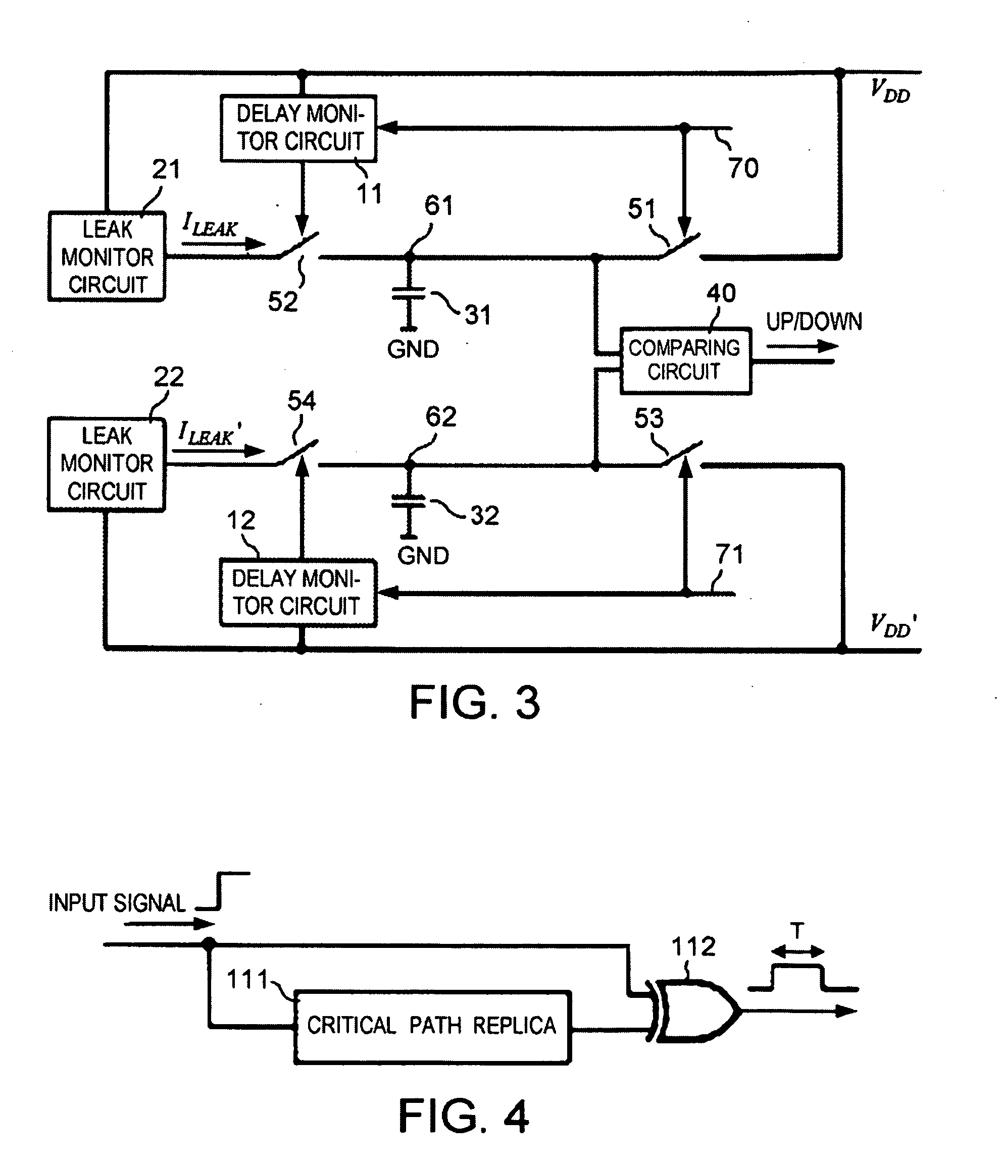
[0019]According to the present invention, a power supply voltage for minimizing the energy consumed by the target circuit is determined, and the target circuit is energized at this power supply voltage. Consequently, the power supply voltage can be controlled to minimize consumed electric power by automatically following a change in an environmental factor. According to the present invention, in particular, a leak monitor circuit which simulates a leak current of the target circuit and a delay monitor circuit which simulates a critical path delay of the target circuit are employed, and a power supply voltage for minimizing the consumed energy is determined based on the leak current and the critical path delay at the time the actual power supply voltage is applied to these monitor circuits. Therefore, the power supply voltage can be controlled optimally without the need for directly measuring the energy consumed by the target circuit itself.

Problems solved by technology

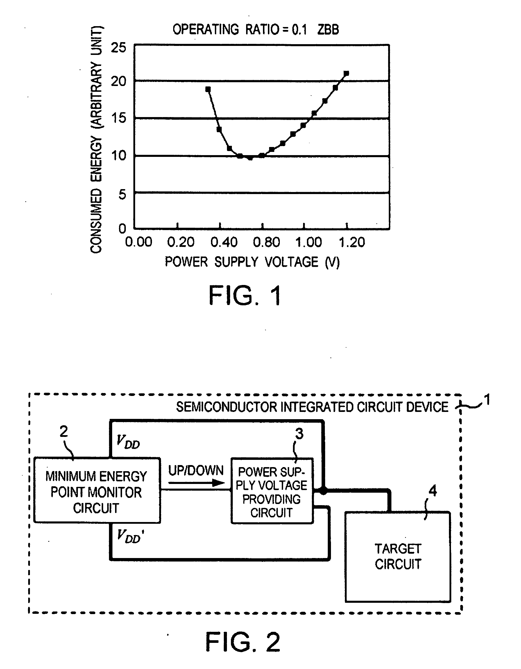
Generally, the power consumed by electronic circuits is monotonously reduced as the power supply voltage is lowered.
However, when the power supply voltage is lowered, the processing capability of the circuit per unit time is also reduced, and hence a problem arises in that the operating time of the circuit for performing the same process is increased.
However, the technology disclosed in WO99 / 12263 does not control the substrate bias voltage for the purpose of minimizing the consumed energy, i.e., the product of the consumed power and the delay time.
However, the technology disclosed in JP-A-2003-115750 does not control the power supply voltage to minimize the consumed energy.
However, the disclosed technology is problematic in that a complex arrangement is required to control both the power supply voltage and the substrate potential, and the energy consumed by the overall circuit at the time the ratio of leak power and switching power is of a target value cannot be said to be minimum.

Method used


Image

  • Semiconductor integrated circuit device and power supply voltage control system
  • Semiconductor integrated circuit device and power supply voltage control system
  • Semiconductor integrated circuit device and power supply voltage control system

Examples


first exemplary embodiment

[0065]A semiconductor integrated circuit device according to a first exemplary embodiment will first be described below.

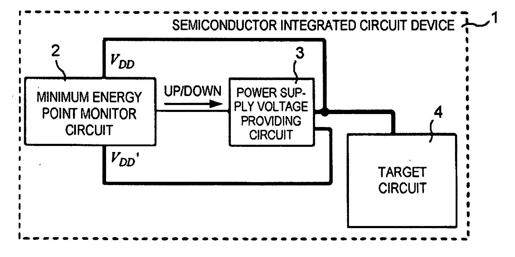
[0066]FIG. 2 shows the overall arrangement of a semiconductor integrated circuit device according to a first exemplary embodiment of the present invention. Semiconductor integrated circuit device 1 includes: target circuit 4 which realizes the primary functions of semiconductor integrated circuit device 1 and performs a process to be performed by semiconductor integrated circuit device 1; minimum energy point monitor circuit 2 which detects a power supply voltage at which the energy consumed by target circuit 4 is minimum, and power supply voltage providing circuit 3 which generates power supply voltage VDD to be supplied to target circuit 4.

[0067]Target circuit 4 is a circuit whose power supply voltage is to be controlled. Power supply voltage providing circuit 3 also generates voltage VDD′ which is lower than power supply voltage VDD by ΔV. Voltages VDD, VDD′ are...

second exemplary embodiment

[0083]A semiconductor integrated circuit device according to a second exemplary embodiment of the present invention will be described below. The semiconductor integrated circuit device of the second exemplary embodiment has an overall arrangement which is similar to the semiconductor integrated circuit device of the first exemplary embodiment shown in FIG. 2, and is different therefrom only as to the circuit arrangement of minimum energy point monitor circuit 2. Therefore, minimum energy point monitor circuit 2 in the second exemplary embodiment will be described below. FIG. 11 shows the circuit arrangement of minimum energy point monitor circuit 2 in the second exemplary embodiment.

[0084]Minimum energy point monitor circuit 2 in the second exemplary embodiment includes: delay monitor circuits 11, 12 which monitor a critical path delay of target circuit 4; leak monitor circuits 21, 23 which monitor a leak current of target circuit 4; capacitor 31; comparing circuit 40; and switches ...

third exemplary embodiment

[0089]A semiconductor integrated circuit device according to a third exemplary embodiment of the present invention will be described below. The semiconductor integrated circuit device of the third exemplary embodiment has an overall arrangement which is similar to the semiconductor integrated circuit device of the first exemplary embodiment shown in FIG. 2, and is different therefrom only as to the circuit arrangement of minimum energy point monitor circuit 2. Therefore, minimum energy point monitor circuit 2 in the third exemplary embodiment will be described below. FIG. 14 shows the circuit arrangement of minimum energy point monitor circuit 2 in the third exemplary embodiment.

[0090]Minimum energy point monitor circuit 2 in the third exemplary embodiment includes: delay monitor circuit 11 which monitors a critical path delay of target circuit 4; leak monitor circuit 21 which monitors a leak current of target circuit 4; capacitors 31, 32; comparing circuit 40; and switches 55A, 55B...


PUM


Abstract

A semiconductor integrated circuit device includes: a target circuit whose at least power supply voltage is variable; a power supply voltage providing circuit feeding the target circuit with a power supply voltage; and a minimum energy point monitor circuit detecting an energy-minimizing power supply voltage which minimizes a change in the energy consumed by the target circuit upon a change in the power supply voltage. The power supply voltage delivered by the power supply voltage providing circuit is controlled so as to be equal to the energy-minimizing power supply voltage detected by the minimum energy point monitor circuit.

Description

TECHNICAL FIELD[0001]The present invention relates to a semiconductor integrated circuit device, and more particularly to a semiconductor integrated circuit device for performing power supply voltage control for reducing the energy consumed by the semiconductor integrated circuit, and a power supply voltage control system based on such control.BACKGROUND ART[0002]One of major tasks to be achieved by mobile devices is an increase in the service life of batteries for powering the mobile devices. As one solution of the task, reduction in the energy consumed by the internal circuit of the mobile devices is required. Since the consumed energy is proportional to the electric power consumed by the internal circuit, efforts have been made to research various low-power technologies for reducing the energy consumption. For reducing the power consumed by semiconductor integrated circuits incorporating CMOS logic gates, it is effective to employ a DVFS (Dynamic Voltage and Frequency Scaling) pr...

Claims


Application Information

Patent Timeline
Patent Type & Authority Applications(United States)
IPC IPC(8): G05F1/10
CPCH03K19/0016
Inventor IKENAGA, YOSHIFUMINOMURA, MASAHIRO
Owner NEC CORP
Learn More