

Substrate treatment apparatus and substrate treatment method
a substrate treatment and substrate technology, applied in the direction of photomechanical equipment, instruments, coatings, etc., can solve the problems of coating film not being uniformized sufficiently, reducing flowability, and coating film being decreased, so as to achieve high accuracy
- Summary
- Abstract
- Description
- Claims
- Application Information
AI Technical Summary
Benefits of technology
Problems solved by technology
Method used
Image

Examples
Embodiment Construction
[0044]Hereinafter, preferred embodiments of the present invention will be described in detail with reference to the accompanying drawings. A case will be described now in which the substrate treatment method according to the present invention is applied to the SOG film forming method for a semiconductor wafer.
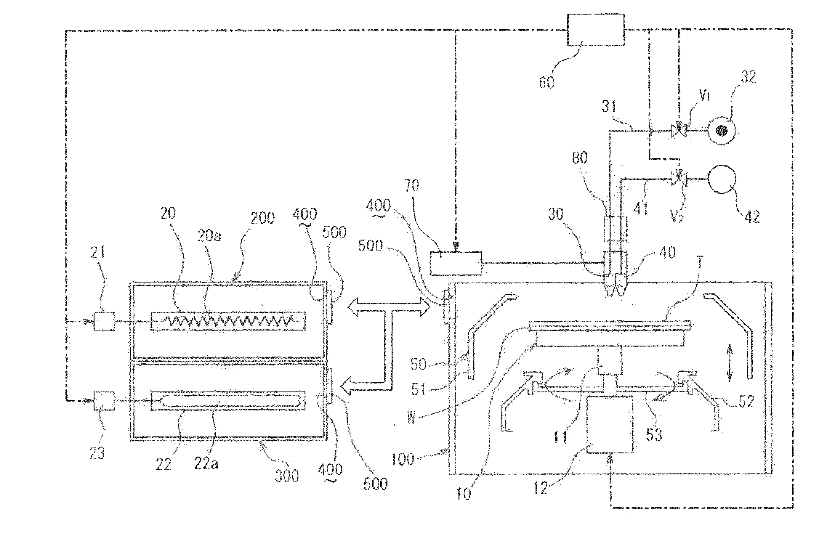
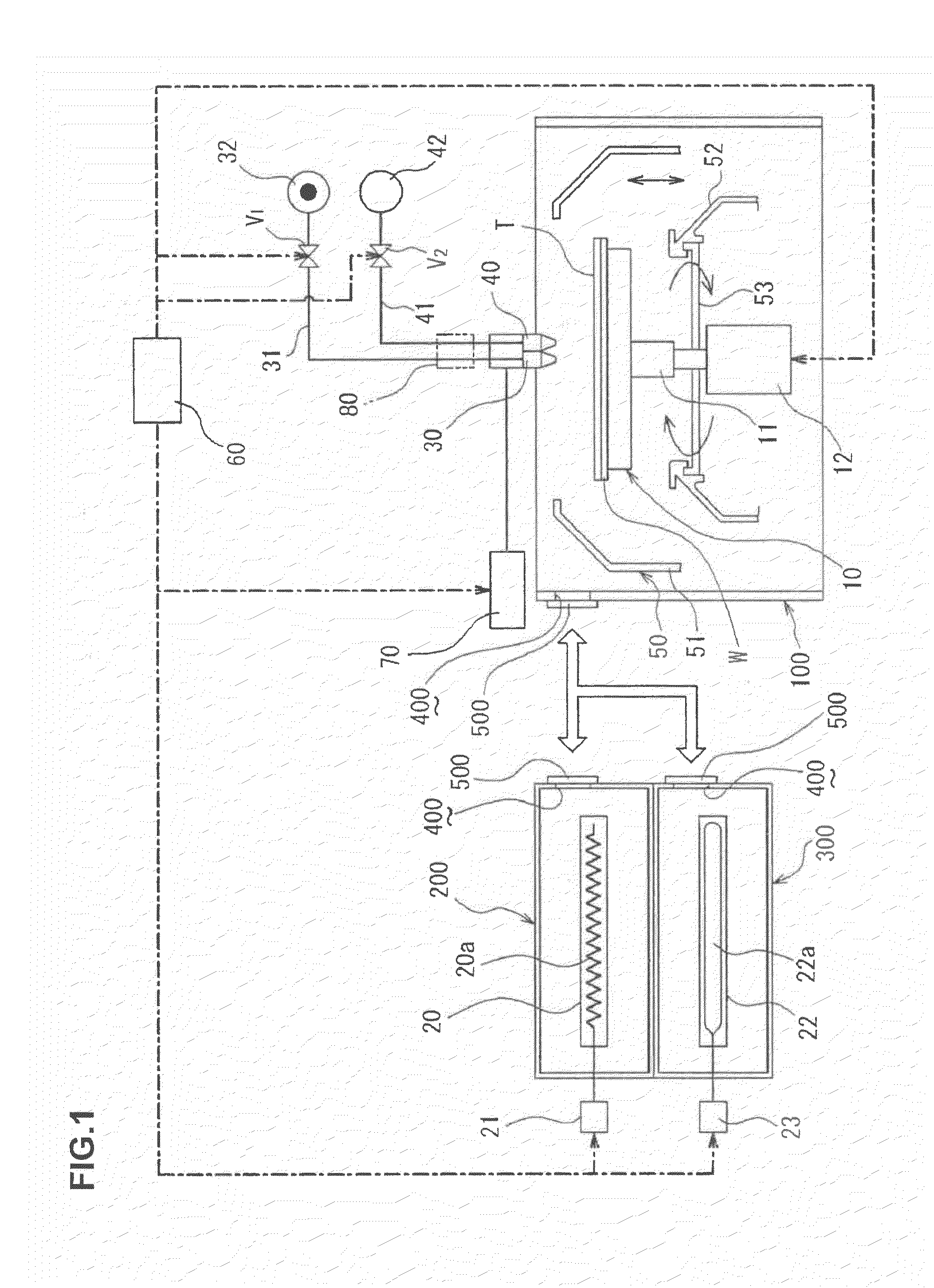
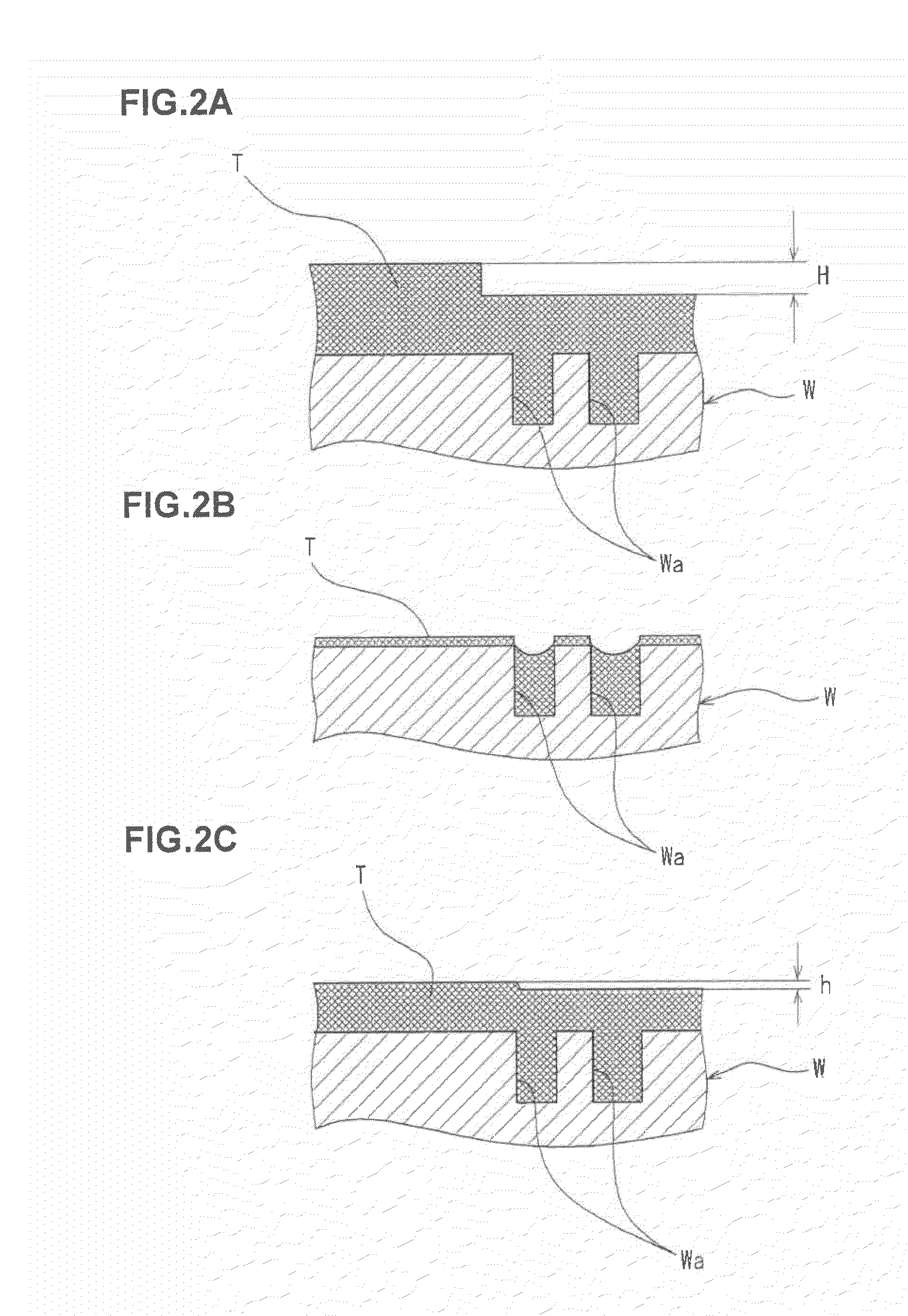
[0045]FIG. 1 is a schematic cross-sectional view showing a first embodiment of a substrate treatment apparatus according to the present invention. The substrate treatment apparatus includes a spin chuck 10 that is a rotating and holding means for holding and horizontally rotating a semiconductor wafer W (hereinafter, referred to as a wafer W) that is a substrate having an uneven surface, a heating means 20 for heating the wafer W to a predetermined temperature, a cooling means 22 for cooling the wafer W heated by the heating means 20, a coating solution supply nozzle 30 for dropping (supplying) an SOG solution, such as polysilazane that is a coating solution onto the front surf...
PUM
| Property | Measurement | Unit |
|---|---|---|
| temperature | aaaaa | aaaaa |
| thickness | aaaaa | aaaaa |
| concentration | aaaaa | aaaaa |
Abstract
Description
Claims
Application Information