

Semiconductor device including dummy gate part and method of fabricating the same
a technology of semiconductor substrate and gate part, which is applied in the direction of semiconductor substrate, electrical apparatus, basic electric elements, etc., can solve the problems of defective pattern and defect pattern in the formation of circuit pattern, and achieve the effect of reducing density difference, facilitating shallow trench isolation operation, and reducing the level difference between certain material layers on semiconductor substra
- Summary
- Abstract
- Description
- Claims
- Application Information
AI Technical Summary
Benefits of technology
Problems solved by technology
Method used
Image

Examples
Embodiment Construction
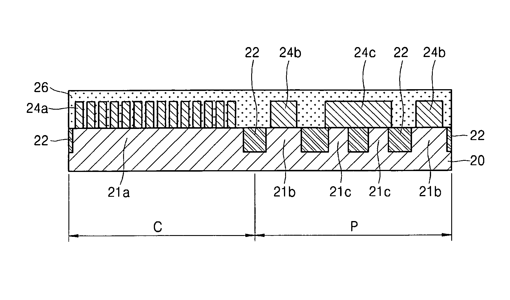
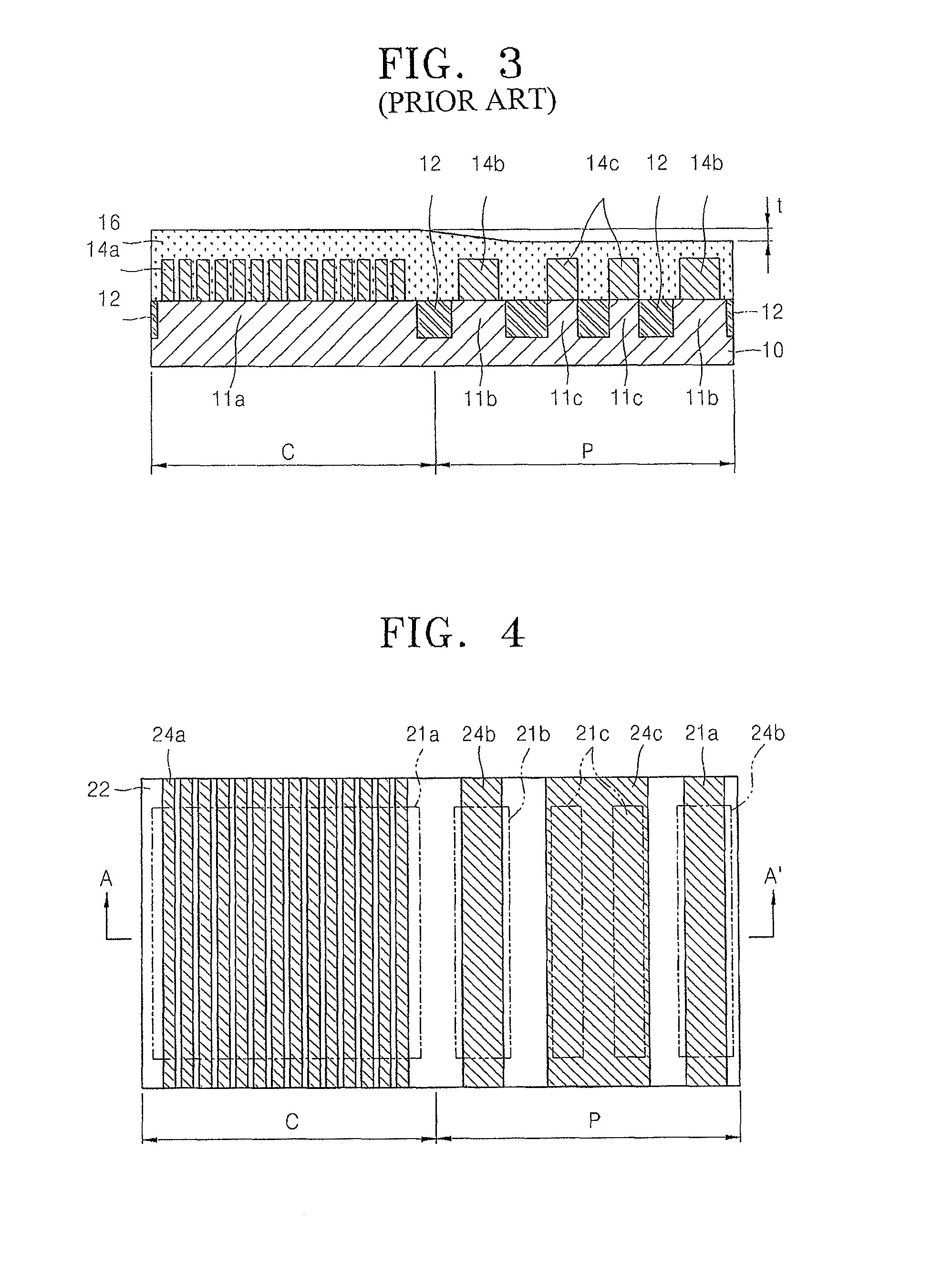
[0036]FIG. 4 is a plan view of a semiconductor device according to an embodiment of the present invention, and FIGS. 5 through 7 are sectional views illustrating a process FOR manufacturing the semiconductor device, taken along line A-A′ of FIG. 4.
[0037]Referring to FIGS. 4 and 5, the top surface of a semiconductor substrate 20, which is, for example, formed of a silicon single crystal, is divided into two regions: a cell region C, on which semiconductor memory devices will be formed, and a peripheral region P, which is formed around the cell region C and on which some control devices and dummy devices will be formed. A real active region 21a, surrounded and defined by a device isolating region 22, is formed in the cell region C. A plurality of dummy active regions 21c, surrounded and defined by the device isolating region 22, are formed in the peripheral region P. Real active regions 21b are also formed in the peripheral region P. When the peripheral region P is formed as a single ...
PUM
 Abstract
Description
Claims
Application Information