Transparent electrode capacitance sensor and process for manufacturing the same

a technology of transparent electrodes and capacitance sensors, which is applied in the direction of resistance/reactance/impedence, instruments, computing, etc., can solve the problems of reduced viewable area of transparent electrodes, increased parasitic capacitance, and complicated manufacturing process, so as to improve the design properties and reliability. , the effect of saving material costs

Active Publication Date: 2016-09-15
SHIN-ETSU POLYMER CO LTD
View PDF3 Cites 6 Cited by
  • Summary
  • Abstract
  • Description
  • Claims
  • Application Information

AI Technical Summary

Benefits of technology

[0021]In accordance with the embodiments of the prevent invention, a transparent electrode capacitance sensor with an excellent reliability and material cost saved, which is excellent in designing properties, secures wide viewable area, and reduces the level difference between the transparent electrode and the auxiliary electrode to suppress bubbling and resultant parasitic capacitance, and a process for manufacturing the same transparent electrode capacitance sensor can be provided.

Problems solved by technology

If the transparent electrode and the auxiliary electrode are intended to be precisely aligned in order to avoid such a variation in the conduction area between the transparent electrode and the auxiliary electrode due to the misalignment, the process for manufacturing the sensor become inevitably complicated.
In a case where the auxiliary electrode is formed of the material which is different from the material for the transparent electrode, as described in Patent Document 1 and Patent Document 2, the problems or drawbacks are as follows: (i) the auxiliary electrode which is disposed at the periphery of the transparent electrode outstands to compromise the appearance or designing properties; (ii) as there is created a great level difference between the transparent electrode and the auxiliary electrode, during the formation of an covering over these transparent and auxiliary electrode, air bubble entrapped in the covering leads to the increase in parasitic capacitance; (iii) due to the auxiliary electrode the viewable area of the transparent electrode is reduced; and (iv) as the material such as silver and gold is expensive, material cost increases.

Method used


Image

  • Transparent electrode capacitance sensor and process for manufacturing the same
  • Transparent electrode capacitance sensor and process for manufacturing the same
  • Transparent electrode capacitance sensor and process for manufacturing the same

Examples


first embodiment

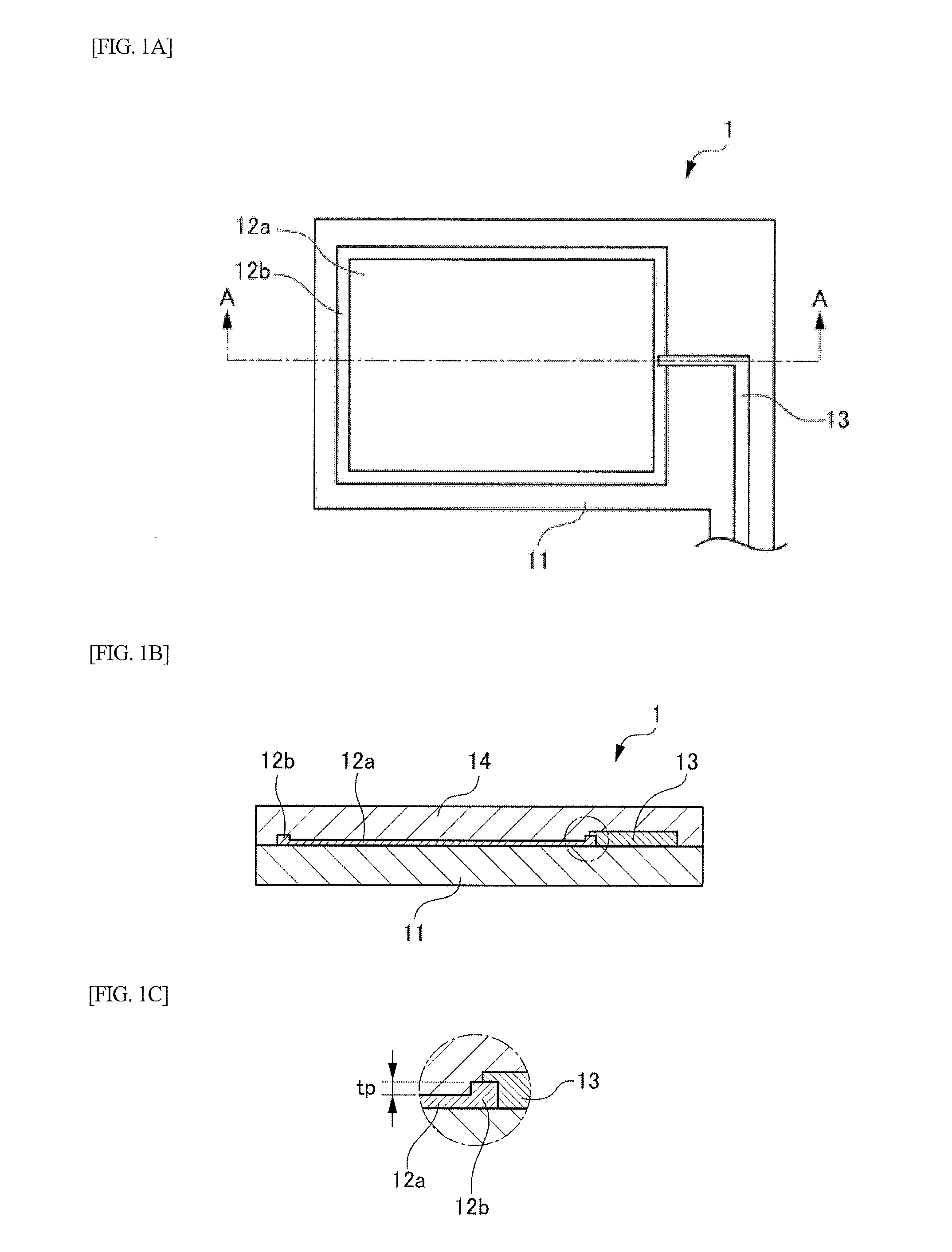
[0059]A first embodiment of a transparent electrode capacitance sensor in accordance with the present invention is hereinafter described. FIG. 1A is a top view of a first embodiment of a transparent electrode capacitance sensor in accordance with the present invention, FIG. 1B is a cross-sectional view of FIG. 1A along the line A-A, and FIG. 1C is an enlarged view of an encircled portion of FIG. 1B.

[0060]The embodiment of the transparent electrode capacitance sensor 1 has a transparent resin substrate 11, a transparent electrode 12a formed on one surface (i.e., single surface) of the transparent resin substrate 11, a pseudo auxiliary electrode 12b formed at the outer periphery of the transparent electrode 12a, a lead wire 13 connected to the pseudo auxiliary electrode 12b at its one end, and an adhesive layer 14 as a top surface as shown in FIG. 1B.

[0061]Referring to FIG. 1C, the pseudo auxiliary electrode 12b has a thickness greater than that of the transparent electrode 12a by a l...

second embodiment

[0083]Next, a transparent electrode capacitance sensor in accordance with a second embodiment of the present invention is described. Since the geometrical configuration and the material for the transparent electrode capacitance sensor in accordance with the second embodiment of the present invention are equal or similar to those for the transparent electrode capacitance sensor in accordance with the first embodiment, description thereof is omitted. The transparent electrode capacitance sensor in accordance with the second embodiment has the geometrical configuration as shown in FIGS. 1A, 1B, and 1C.

[0084]The process for manufacturing the transparent electrode capacitance sensor in accordance with the second embodiment of the present invention will be described with reference to FIGS. 1A, 1B, 1C, and 6. FIG. 6 is a flow chart of a process for manufacturing the second embodiment of a transparent electrode capacitance sensor in accordance with the present invention.

21 (S21)>

[0085]In th...

third embodiment

[0095]Next, a transparent electrode capacitance sensor in accordance with a third embodiment of the present invention will be described. FIG. 8A is a top view of a third embodiment of a transparent electrode capacitance sensor in accordance with the present invention, and FIG. 8B is a cross-sectional view of FIG. 8A along the line A-A.

[0096]A transparent electrode capacitance sensor 1 has a transparent resin substrate 11, a transparent electrode 12a formed on one surface of the transparent resin substrate 11, a pseudo auxiliary electrode 12b formed at the outer periphery of the transparent electrode 12a, a lead wire 13 connected to the pseudo auxiliary electrode 12b at its one end and interposed between the pseudo auxiliary electrode 12b and the transparent resin substrate 11, and an adhesive layer 14 as a top surface as shown in FIG. 8B. The properties, material, preferred thickness and etc. of the transparent resin substrate 11 and the transparent electrode 12a of third embodiment...


PUM

PropertyMeasurementUnit
thicknessaaaaaaaaaa
thicknessaaaaaaaaaa
thicknessaaaaaaaaaa

Abstract

A transparent electrode capacitance sensor includes a transparent resin substrate; at least one transparent electrode formed on the transparent resin substrate; a pseudo auxiliary electrode formed in at least a portion of an outer periphery of the transparent electrode; and a lead wire connected to the pseudo auxiliary electrode, wherein the pseudo auxiliary electrode is thicker than the transparent electrode, and includes the same material as the transparent electrode.

Description

TECHNICAL FIELD[0001]The present invention relates to a transparent electrode capacitance sensor and a process for manufacturing the transparent electrode capacitance sensor.BACKGROUND ART[0002]A detection of a touch sensor includes a capacitance-type detection which responds to an electric power which flows through a finger in contact with a screen to transform the motion of the finger into an operation command. There is disclosed a capacitance sensor using such a capacitance-type detection in which an auxiliary electrode having an electric resistance lower than that of a transparent electrode is formed in at least a portion of the periphery of the transparent electrode so as to suppress a variation in detection sensitivity. For more detail, see, for example, Patent Document 1.[0003]However, in a case where misalignment between the transparent electrode and the auxiliary electrode occurs during the manufacture of the sensor as disclosed in Patent Document 1, the conduction area bet...

Claims


Application Information

Patent Timeline
Patent Type & Authority Applications(United States)
IPC IPC(8): G06F3/041G06F3/044
CPCG06F3/0416G06F3/044G06F2203/04102G06F2203/04112G06F2203/04103G06F3/0443G01R27/00
Inventor NOZAKI, TOMOHIROKOMATSU, HIROTOKAWAMURA, TAKASHI
Owner SHIN-ETSU POLYMER CO LTD
Why Eureka
Try Eureka