Semiconductor integrated circuit device

a technology of integrated circuit and semiconductor, which is applied in the direction of semiconductor devices, semiconductor/solid-state device details, electrical apparatus, etc., can solve the problems of reducing the operating withstand voltage, generating the dependency of delayed time on a frequency, and kinks

Inactive Publication Date: 2011-02-10
RENESAS ELECTRONICS CORP
View PDF10 Cites 15 Cited by
  • Summary
  • Abstract
  • Description
  • Claims
  • Application Information

AI Technical Summary

Benefits of technology

[0024]There is provided a semiconductor integrated circuit device, which is provided on an SOI substrate and includes an input / output circuit section and a core circuit section and in which a power-supply voltage of the input / output circuit section is higher than a power-supply voltage of the core circuit section, wherein deterioration in characteristic caused by a substrate flotation effect of a MOS transistor constituting the input / output circuit section can be prevented.
[0026]As thus described, in an input / output circuit section, a first finger length of a first gate electrode of a first MOS transistor, which is defined by a length of a portion on an active region, is set shorter than a second finger length of a second gate electrode of the second MOS transistor, which is defined by a length of a portion on an active region. Therefore, ever when a collisional ionization phenomenon apparently occurs at a drain end of the MOS transistor, it is possible in the input / output circuit section to which a higher power supply voltage is supplied than the core circuit section to suppress a substrate floatation effect with reliability, so as to prevent deterioration in transistor characteristic caused by the substrate floatation effect.
[0028]As thus described, in an input / output circuit section, the maximum finger length among respective finger lengths of a plurality of kinds of MOS transistors in a first group is set shorter than the maximum finger length among respective finger lengths of a plurality of kinds of MOS transistors in a second group. Therefore, in a case where a plurality of kinds of MOS transistor having different finger lengths are provided within the same one circuit, even when a collisional ionization phenomenon apparently occurs at a drain end of the MOS transistors, it is possible in the input / output circuit section to which a higher power supply voltage is supplied than the core circuit section to suppress a substrate floatation effect with reliability, so as to prevent deterioration in transistor characteristic caused by the substrate floatation effect.

Problems solved by technology

However, there have been a variety of problems generated by a substrate floatation effect, including a problem in that carriers (holes in NMOS) generated by a collisional ionization phenomenon remain in a body region including a channel formation region, thereby to cause generation of a kink, reduction in operating withstand voltage, and generation of dependency of delayed time on a frequency due to an unstable potential of the body region.
However, in the case of adopting the PTI structure, when the channel width of the MOS transistor is increased without restriction, the body region under the gate electrode becomes longer, resulting in that body resistance increases to make it difficult to fix a potential of the body region, leading to a problem of deterioration in transistor characteristic caused by the substrate floatation effect.
As thus described, there has been a problem in the SOI device with the SOI structure adopted therein in that the length of the MOS transistor in the channel width direction cannot be increased from the aspect of suppressing deterioration in transistor characteristic, and it has not been possible to solve the problem by a conventional design index of arranging gate electrodes in parallel to avoid restriction on area.

Method used


Image

  • Semiconductor integrated circuit device
  • Semiconductor integrated circuit device
  • Semiconductor integrated circuit device

Examples


embodiment

A. Regarding Fixing of Potential of Body Region

[0037]First, fixing of a potential of a body region in an SOI device with the PTI structure adopted therein is described using FIGS. 1 and 2.

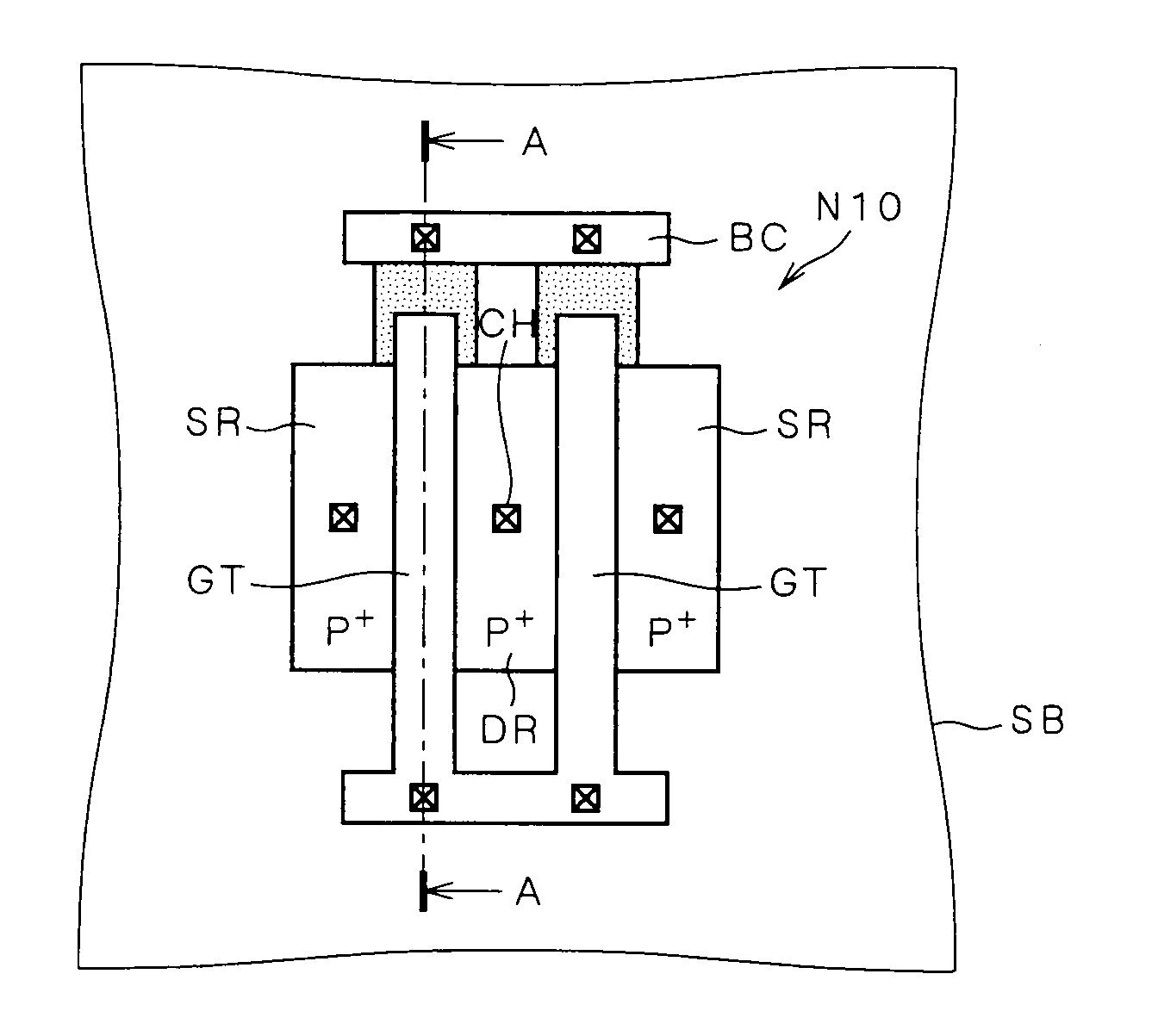
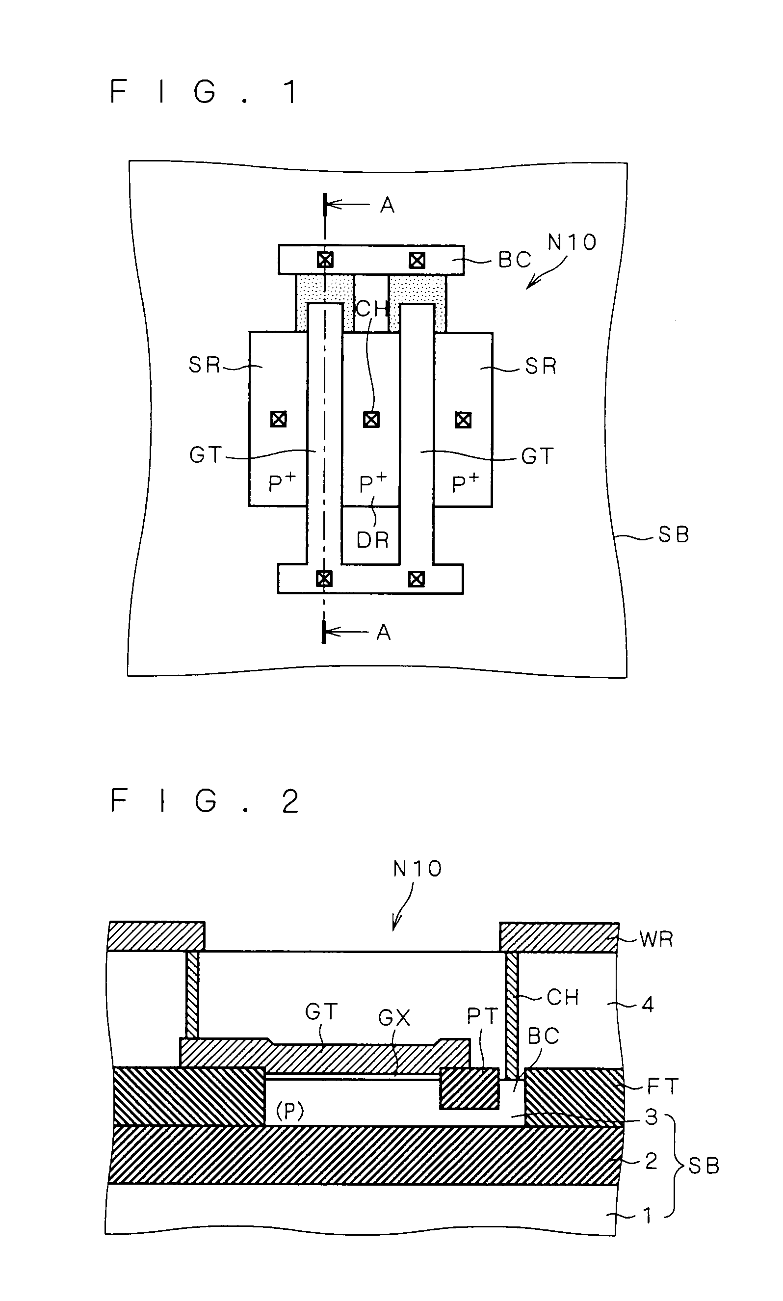
[0038]FIG. 1 is a view showing a plane configuration of αα MOS transistor (NMOS transistor) N10 with the PTI structure adopted therein. FIG. 2 is a sectional view on arrow A-A of FIG. 1. In FIG. 1, two gate electrodes GT are provided in parallel in a gate length direction on an SOI substrate SB. A drain region DR in which P-type impurities have been introduced is provided between the two gate electrodes GT within the surface of the SOI substrate SB. The source region SR in which the P-type impurities have been introduced is provided on the outside side surface of the gate electrode GT on the opposite side to the drain region DR within the surface of the SOI substrate SB.

[0039]A body contact region BC is provided on the outside of one end of the two gate electrodes GT in a gate width direction, in a...


PUM


Abstract

A finger length al of a transistor P11 is longer than a finger length Al of a transistor P1, and a finger length b1 of a transistor N11 is longer than a finger length B1 of a transistor N1. The finger length b1 of the transistor N11 is shorter than the finger length A1 of the transistor P1, and the relation: a1>A1>b1>B1 is established. In a relation between an I / O section and a logic circuit section, as for MOS transistor of the same conductive type, a finger length of a MOS transistor constituting the logic circuit section is set so as to be longer than a finger length of a MOS transistor constituting the I / O section.

Description

CROSS-REFERENCE TO RELATED APPLICATIONS[0001]This application is a divisional of U.S. application Ser. No. 11 / 733,351, filed Apr. 10, 2007, the entire contents of which are incorporated herein by reference, and is based upon and claims the benefit of priority from prior Japanese Patent Application No. 2006-109733, filed Dec. 4, 2006.BACKGROUND OF THE INVENTION[0002]1 . Field of the Invention[0003]The present invention relates to a semiconductor integrated circuit device, and particularly relates to a semiconductor integrated circuit device provided on an SOI substrate.[0004]2. Description of the Background Art[0005]In a current semiconductor integrated circuit device (LSI) having a plurality of circuit sections with different functions, such as an input / output circuit (I / O) section, a logic circuit section and a memory section, a configuration is adopted where a plurality of voltages are supplied from external power supplies.[0006]For example, an LSI with two power supplies has been...

Claims


Application Information

Patent Timeline
Patent Type & Authority Applications(United States)
IPC IPC(8): H01L27/118
CPCH01L27/1203H01L27/0207
Inventor IWAMATSU, TOSHIAKI
Owner RENESAS ELECTRONICS CORP
Why Eureka
Try Eureka