Method for forming transparent organic electrode

a technology of organic electrodes and transparent electrodes, which is applied in the direction of organic semiconductor devices, coatings, semiconductor devices, etc., can solve the problems of high processing costs, low manufacturing yield of transparent electrodes, and crack generation on the sections of transparent electrodes, so as to achieve good transparency, reduce the effect of consuming less raw materials and low defect ra

Inactive Publication Date: 2011-03-10
SAMSUNG ELECTRO MECHANICS CO LTD
View PDF8 Cites 4 Cited by
  • Summary
  • Abstract
  • Description
  • Claims
  • Application Information

AI Technical Summary

Benefits of technology

[0011]An aspect of the present invention provides a method for forming a transparent organic electrode with good transparency while less consuming less raw materials and having a low rate of defectivity.

Problems solved by technology

However, the process of coating the metal oxides on the substrate requires a vacuum, incurring high processing costs.
However, the rate of crack generation on the sections of the transparent electrodes, namely, in the edges of the unit cells, due to mechanical stress applied thereto during the cutting process is so high that the manufacturing yield of the transparent electrode is very low.
In addition, attaching the electrode to the transparent conductive material having the metal oxide conductive layer necessarily accompanies a process of removing the conductive layer from a portion on which an electrode is to be attached, increasing the manufacturing cost thereof.

Method used


Image

  • Method for forming transparent organic electrode
  • Method for forming transparent organic electrode
  • Method for forming transparent organic electrode

Examples


embodiment 1

[0074]In order to check for variations in resistance according to the temperature for thermally treating the organic conductive composition, the organic conductive composition was printed for 30 minutes by using inkjet printing, screen printing, Gravure printing, or offset printing, and then the resistance values according to the respective temperatures of thermal treatments were compared.

[0075]FIG. 3a is a graph of variations of resistance values over temperature of thermal treatment based on various printing methods.

[0076]It is noted that when the organic conductive composition was printed through various printing methods and then thermally heated within the temperature range from 25° C. to 150° C., the resistance of unit cells including the organic conductive composition was not greatly increased, while the resistance was sharply increased as the temperature went beyond 150° C.

[0077]Namely, it is noted that, according to an exemplary embodiment of the present invention, when the ...

embodiment 2

[0078]In order to check crack generation rates according to the temperatures of thermal treatment of the organic conductive composition, the organic conductive composition was printed by using inkjet printing, screen printing, Gravure printing, or offset printing, and then the crack generation rates according to the respective temperatures of thermal treatments were compared.

[0079]In the case that the crack generation rate (A) is based on the ratio of the length of a crack per unit length when the crack is generated in a unit area, the more cracks that are generated, the larger the crack generation rate value.

[0080]Crack generation rate=length of crack / unit length.

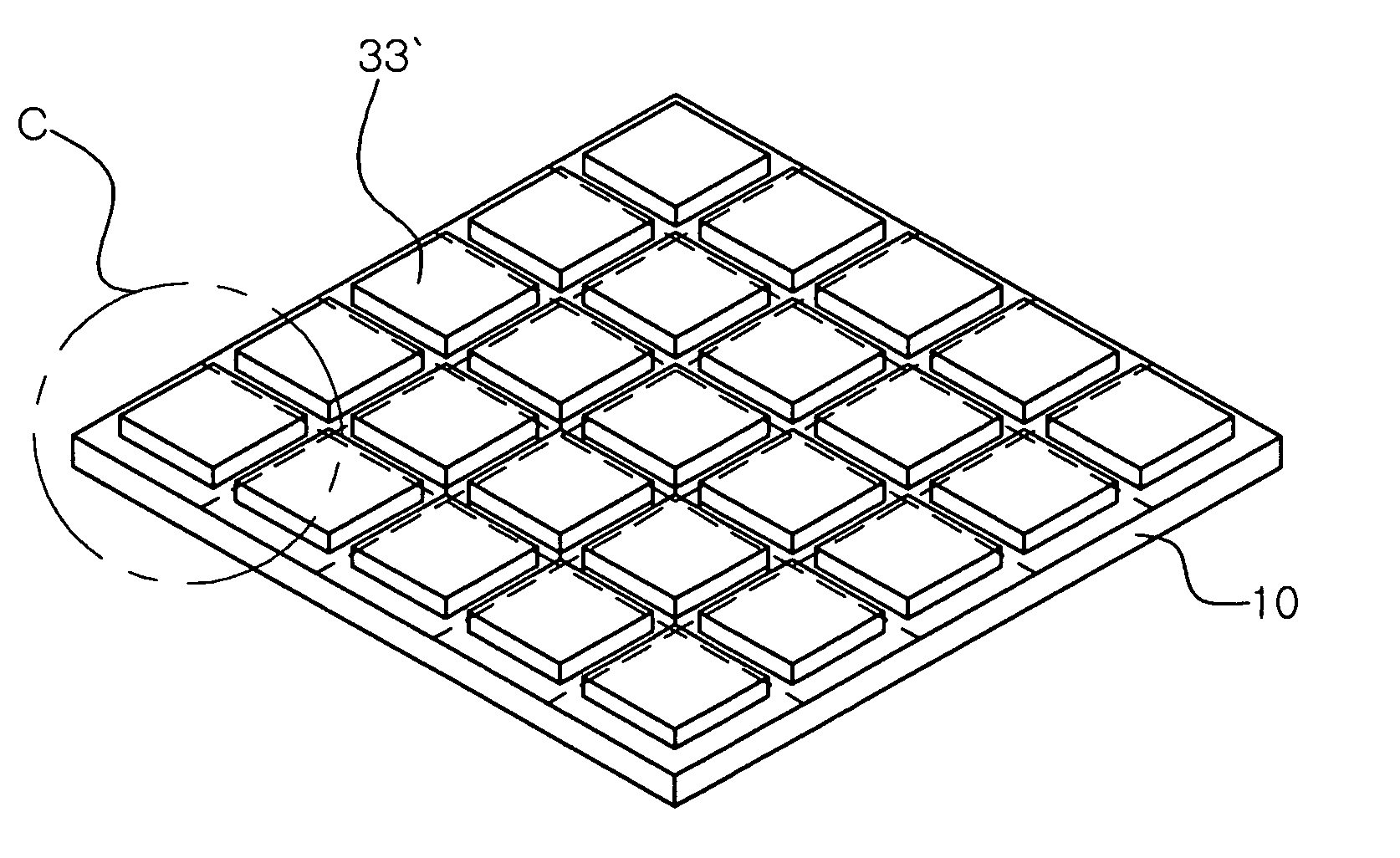
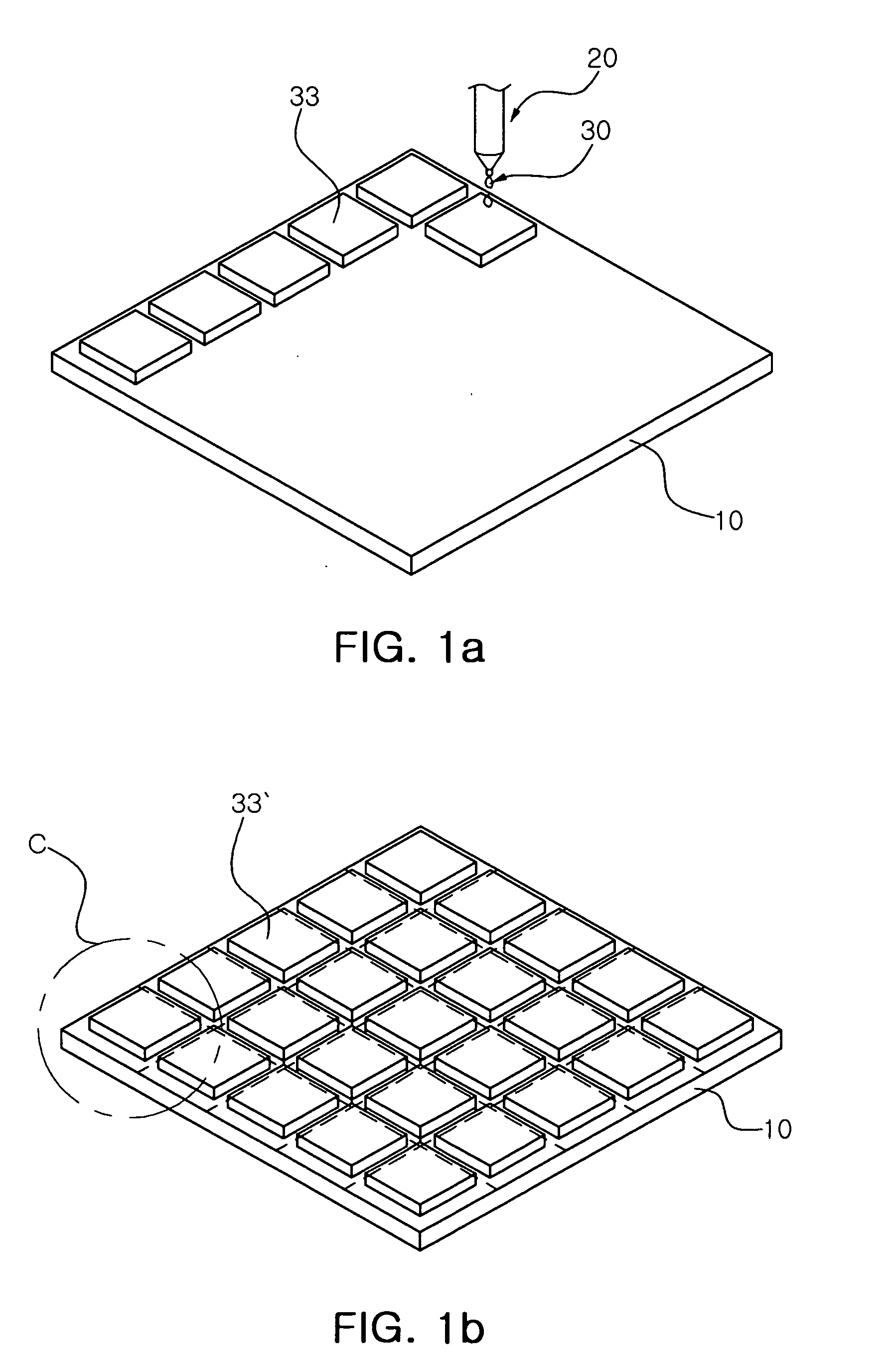
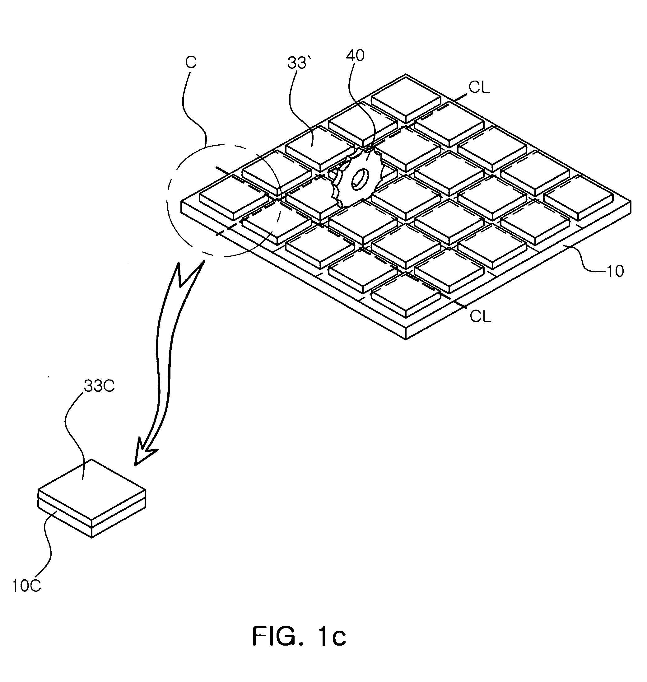
[0081]With reference to FIG. 3b, When the cutting lines were formed to demarcate the cells according to an exemplary embodiment of the present invention and conductive patterns within the cells demarcated by the cutting lines were thermally treated, a crack generation rate did not exceed 0.5 although any printing method wa...


PUM

PropertyMeasurementUnit
temperatureaaaaaaaaaa

Abstract

A method for forming a transparent organic electrode includes: preparing an organic conductive composition including a conductive material, a binder, and a solvent; preparing a substrate on which cutting lines demarcating cells are formed; forming a conductive layer by printing a conductive pattern within each of the cells demarcated by the cutting lines by using the organic conductive composition; and dicing the substrate along the cutting lines to separate the cells each having the conductive layer formed thereon. A transparent organic electrode can be formed with good transparency while consuming less raw materials and having a low defectivity rate.

Description

CROSS-REFERENCE TO RELATED APPLICATIONS[0001]This application claims the priority of Korean Patent Application Nos. 10-2009-0084210 filed on Sep. 7, 2009, and 10-2010-0082121 filed on Aug. 24, 2010, in the Korean Intellectual Property Office, the disclosures of which are incorporated herein by reference.BACKGROUND OF THE INVENTION[0002]1. Field of the Invention[0003]The present invention relates to a method for forming a transparent organic electrode and, more particularly, to a method for forming a transparent organic electrode with good transparency while consuming less raw materials and having a low rate of defectivity.[0004]2. Description of the Related Art[0005]As computers, various home appliances, and communications devices are being digitalized and rapidly advancing to have increasingly high performance, the implementation of large-scale portable displays is urgently required. In order to implement a large-scale flexible portable display, a display material that can be bent ...

Claims


Application Information

Patent Timeline
Patent Type & Authority Applications(United States)
IPC IPC(8): B05D5/12
CPCH01L51/0022H01L2251/566H01L51/5203H01L51/0037H10K71/611H10K85/1135H10K50/805H10K71/851
Inventor LEE, JONG YOUNGOH, YONGSOOBAEK, YOUNG KIPARK, HO JOON
Owner SAMSUNG ELECTRO MECHANICS CO LTD
Why Eureka
Try Eureka