

Integrated circuit packaging system with a leaded package and method of manufacture thereof
- Summary
- Abstract
- Description
- Claims
- Application Information
AI Technical Summary
Benefits of technology
Problems solved by technology
Method used
Image

Examples
first embodiment
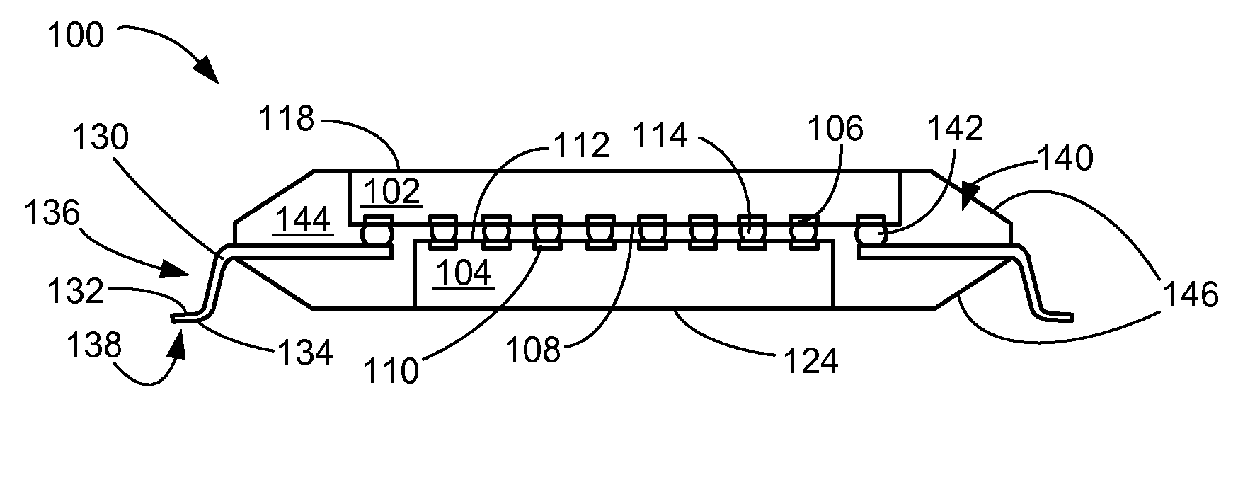
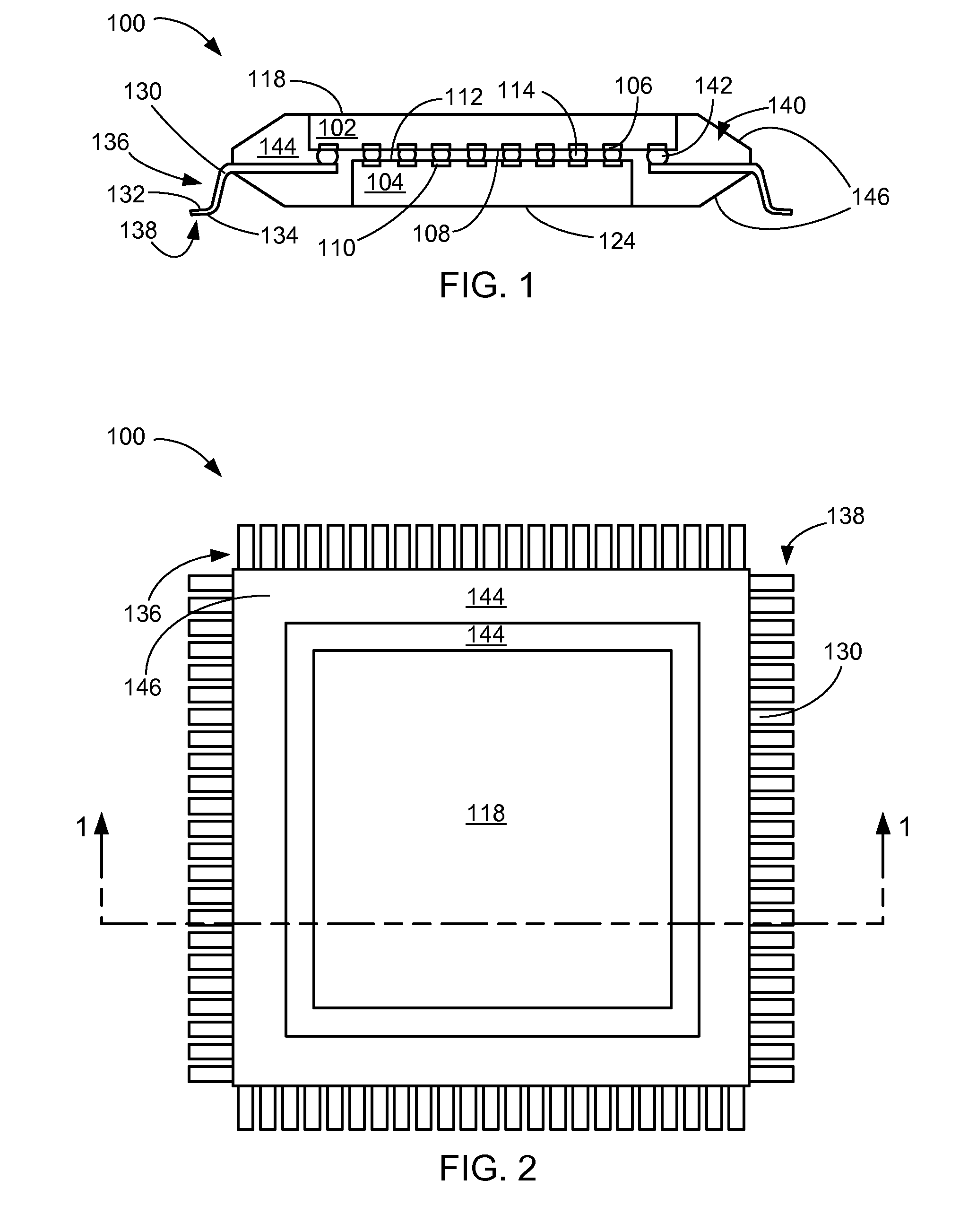
[0026]Referring now to FIG. 1, therein is shown a cross-sectional view of an integrated circuit packaging system 100 in the present invention taken along a line 1-1 of FIG. 2. The integrated circuit packaging system 100 can preferably include a first device 102, such as a flip chip, a wafer level chip scale package (WLCSP), or an integrated circuit device, connected over a second device 104.
[0027]The first device 102 can preferably have planar dimensions greater than planar dimensions of the second device 104, such as a stacked flip chip, a WLCSP, or an integrated circuit device. A thickness of the first device 102 can be different from a thickness of the second device 104. A planar center of the first device 102 can be vertically aligned with a planar center of the second device 104.
[0028]First device connectors 106, such as pads or contacts on a first inward side 108 of the first device 102, can connect to second device connectors 110 on a second inward side 112 of the second devi...
second embodiment
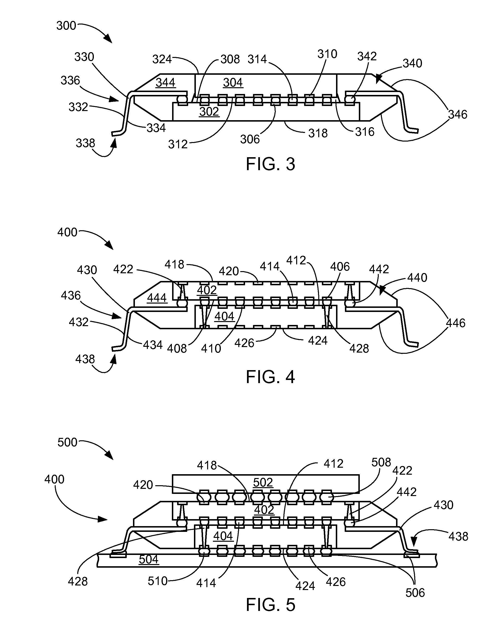
[0045]Referring now to FIG. 3, therein is shown a cross-sectional view of an integrated circuit packaging system 300 in the present invention. The integrated circuit packaging system 300 can preferably include a first device 302, such as a flip chip, a WLCSP, or an integrated circuit device, connected over a second device 304.
[0046]The first device 302 can preferably have planar dimensions greater than planar dimensions of the second device 304, such as a stacked flip chip, a WLCSP, or an integrated circuit device. A thickness of the first device 302 can be different from a thickness of the second device 304. A planar center of the first device 302 can be vertically aligned with a planar center of the second device 304.
[0047]First device connectors 306, such as pads or contacts on a first inward side 308 of the first device 302, can connect to second device connectors 310 on a second inward side 312 of the second device 304. The first device connectors 306, used to provide connectiv...
third embodiment
[0059]Referring now to FIG. 4, therein is shown a cross-sectional view of an integrated circuit packaging system 400 in the present invention. The integrated circuit packaging system 400 can preferably include a first device 402, such as a flip chip, a WLCSP, or an integrated circuit device, connected over a second device 404.
[0060]The first device 402 can preferably have planar dimensions greater than planar dimensions of the second device 404, such as a stacked flip chip, WLCSP, or an integrated circuit device. A thickness of the first device 402 can be different from a thickness of the second device 404. A planar center of the first device 402 can be vertically aligned with a planar center of the second device 404.
[0061]First device connectors 406, such as pads or contacts on a first inward side 408 of the first device 402, can connect to second device connectors 410 on a second inward side 412 of the second device 404. The first device connectors 406, used to provide connectivit...
PUM
 Abstract
Description
Claims
Application Information