Integrated circuit package and process for fabricating the same

a technology of integrated circuits and manufacturing processes, which is applied in the direction of semiconductor devices, electrical equipment, semiconductor/solid-state device details, etc., can solve the problems of limiting the packaging density of such prior art devices, and achieve the effects of reducing manufacturing costs, improving thermal characteristics of the package, and reducing the occurrence of mold flash contamination

Active Publication Date: 2006-08-15
UTAC HEADQUARTERS PTE LTD
View PDF81 Cites 122 Cited by
  • Summary
  • Abstract
  • Description
  • Claims
  • Application Information

AI Technical Summary

Benefits of technology

[0009]In a particular aspect, the external contacts are solder balls that provide package standoff from the motherboard after assembly. This improves thermal characteristics of the package as thermal cycling of the package is less likely to cause fatigue failure of solder joints to the motherboard. Also, the solder balls facilitize reworking of the motherboard assembly by allowing for package removal and replacement or re-attachment to the motherboard without the addition of further solder.
[0010]During fabrication, the leadframe strip is releasably clamped in a mold by releasably clamping the contact pads, followed by molding in the molding compound. Thus, during molding, the contact pads are protected from mold flash contamination, a significant problem in prior art packages. This obviates the need for the use of deflash tape that is placed on the strip before molding to reduce the occurrence of mold flash contamination, thereby reducing manufacturing cost. Also, the need for deflash abrasion of the package is obviated.
[0011]In a particular embodiment, the die sits in a portion of the die attach pad that is reduced in thickness and therefore the length of the wire bonds can be reduced. Also, the wire bonds are lower in the profile of the package, which allows for reduction of the integrated circuit package profile.
[0012]Also, the profile of the mold used in molding the package varies. Thus, the thickness of the molding compound is not uniform in the resulting package. Also, the molding compound is not continuous. The molding compound is broken up by the contact pads, where molding compound flows between but does not cover portions of the contact pads. This reduces the stress caused by mismatch in the coefficients of thermal expansion between the molding compound and the leadframe, in comparison with prior art packages.

Problems solved by technology

The inner leads terminate in outer leads that are bent down to contact a mother board, thereby limiting the packaging density of such prior art devices.

Method used


Image

  • Integrated circuit package and process for fabricating the same
  • Integrated circuit package and process for fabricating the same
  • Integrated circuit package and process for fabricating the same

Examples


Embodiment Construction

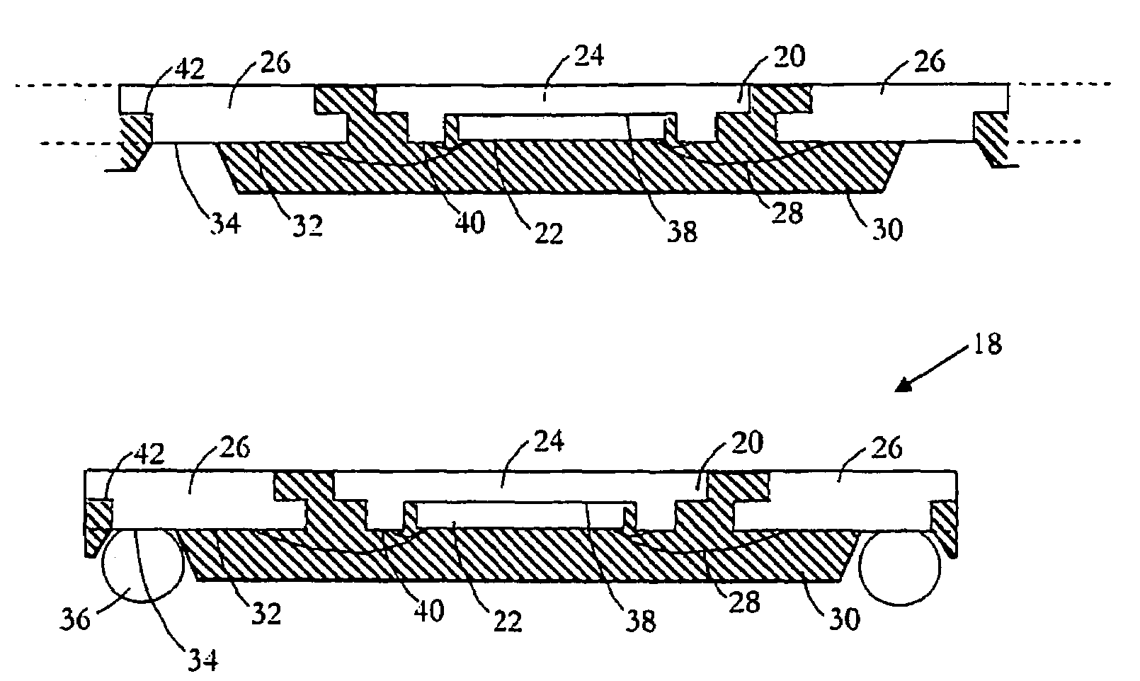
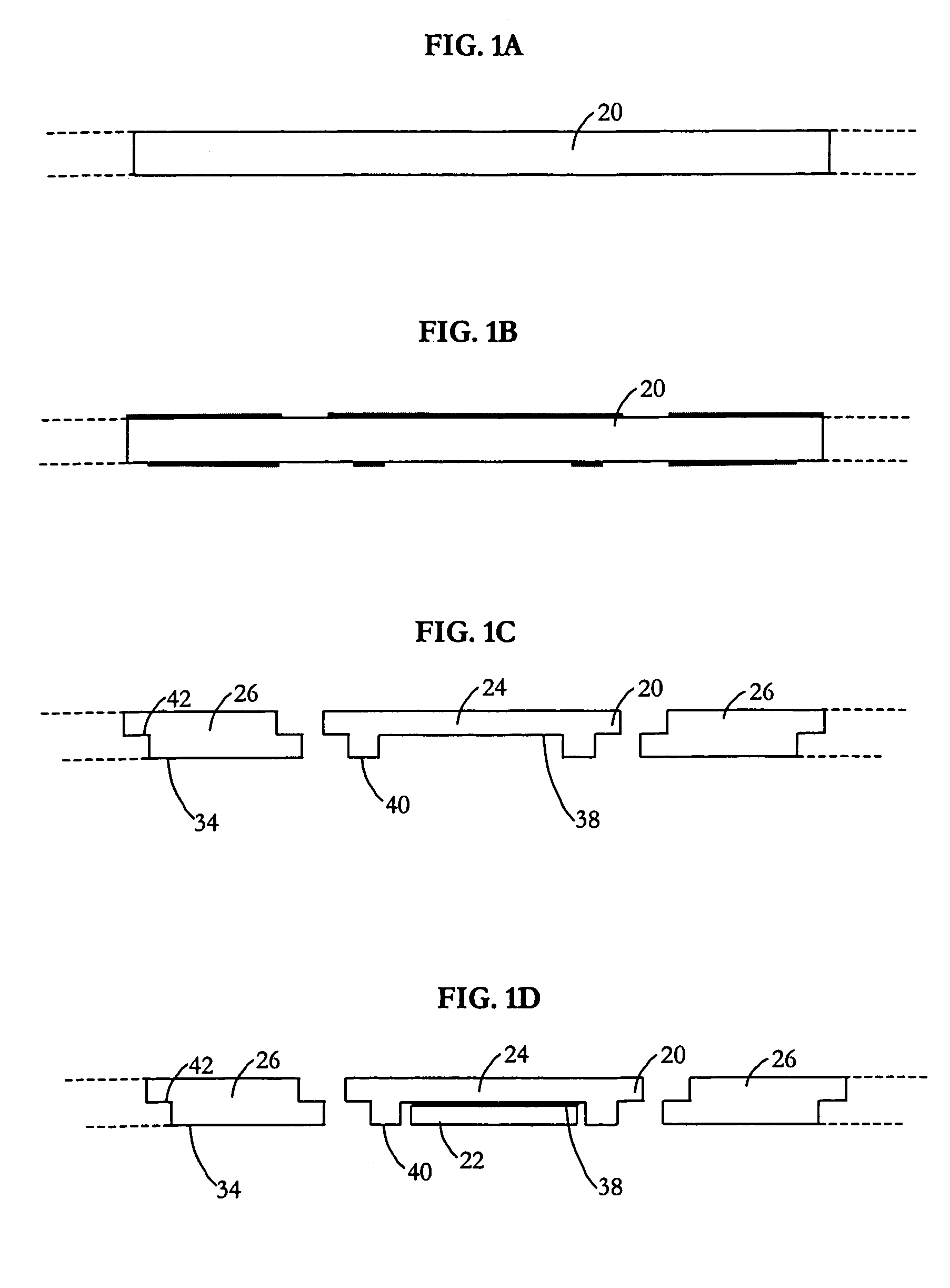
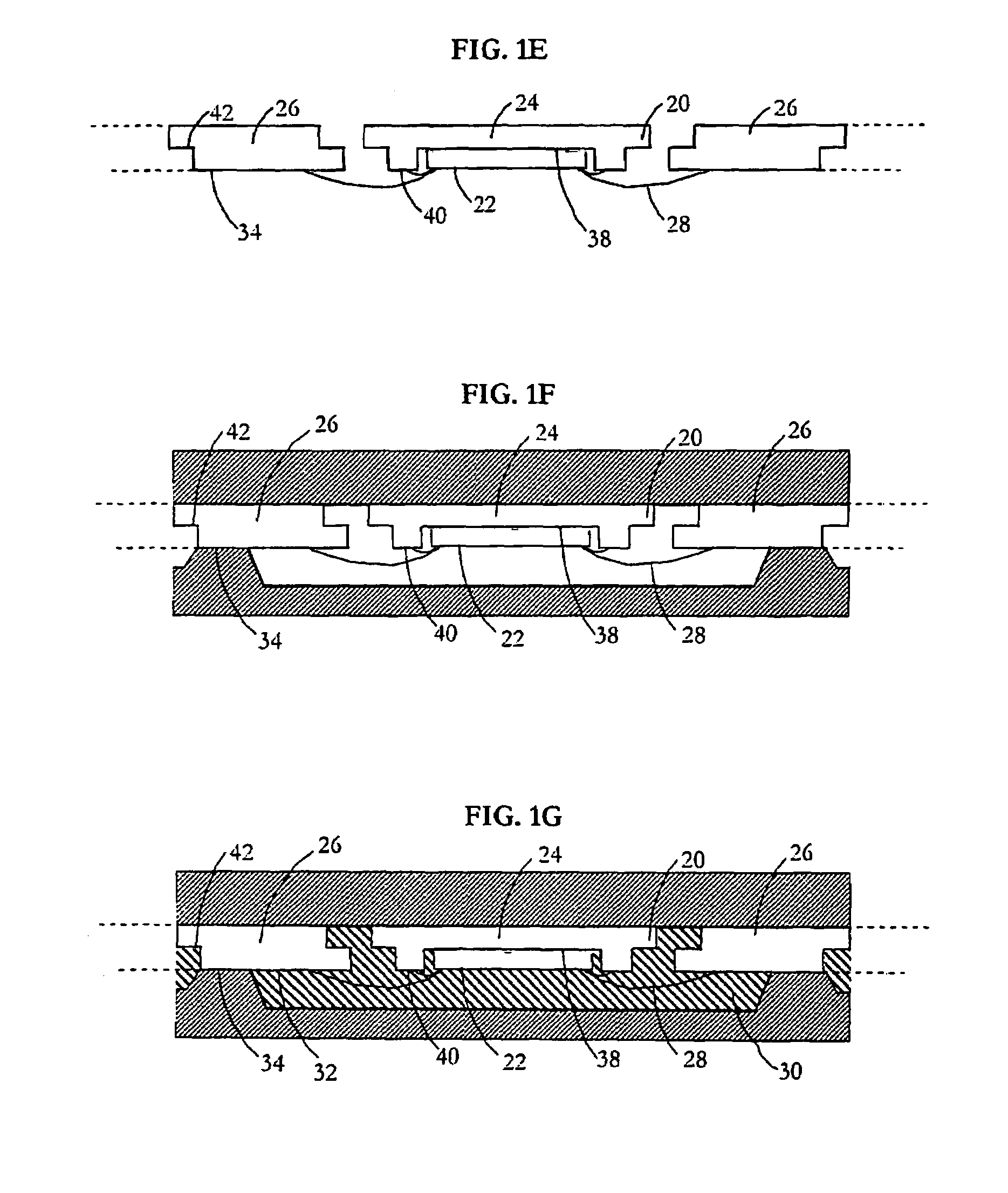
[0015]Reference is made to the Figures to describe a process for fabricating an integrated circuit package according to an embodiment of the present invention. The integrated circuit package is indicated generally by the numeral 18 and includes a semiconductor die 22 mounted to a die attach pad 24 and at least one row of contact pads 26 circumscribing the die attach pad 24. Wire bonds 28 are then bonded to connect the semiconductor die 22 to ones of the contact pads 26. A molding compound 30 covers one side of the semiconductor die 22, the wire bonds 28 and a portion 32 of one side of the contact pads 26 such that a remaining portion 34 of the one side of the contact pads 26 is uncovered and an opposing side of the contact pads 26 is uncovered. External contacts 36 are disposed on the one side of the contact pads 26, at the uncovered remaining portion 34, such that the external contacts 36 protrude from the molding compound 30.

[0016]The integrated circuit package 18 will now be desc...


PUM


Abstract

A process for fabricating an integrated circuit package includes: selectively etching a leadframe strip to define a die attach pad and at least one row of contact pads; mounting a semiconductor die to one side of the leadframe strip, on the die attach pad; wire bonding the semiconductor die to ones of the contact pads; releasably clamping the leadframe strip in a mold by releasably clamping the contact pads; molding in a molding compound to cover the semiconductor die, the wire bonds and a portion of the contact pads not covered by the clamping; releasing the leadframe strip from the mold; depositing a plurality of external contacts on the one side of the leadframe strip, on the contact pads, such that the external contacts protrude from the molding compound; and singulating to provide the integrated circuit package.

Description

FIELD OF THE INVENTION[0001]The present invention relates in general to integrated circuit packaging and more particularly to a process for fabricating an improved integrated circuit package.BACKGROUND OF THE INVENTION[0002]According to well known prior art IC (integrated circuit) packaging methodologies, semiconductor dice are singulated and mounted using epoxy or other conventional means onto respective die attach pads (attach paddles) of a leadframe strip. Traditional QFP (Quad Flat Pack) packages incorporate inner leads which function as lands for wire bonding the semiconductor die bond pads. These inner leads typically require mold locking features to ensure proper positioning of the leadframe strip during subsequent molding to encapsulate the package. The inner leads terminate in outer leads that are bent down to contact a mother board, thereby limiting the packaging density of such prior art devices.[0003]In order to overcome these and other disadvantages of the prior art, th...

Claims


Application Information

Patent Timeline
Patent Type & Authority Patents(United States)
IPC IPC(8): H01L23/495H01L23/48H01L23/485H01L23/498H01L23/52H01L29/40
CPCH01L21/4828H01L23/49503H01L23/49548H01L2224/45144H01L2223/6611H01L2224/48091H01L2224/48247H01L2924/01079H01L2924/15311H01L2924/1532H01L2924/3011H01L2224/32257H01L2224/45124H01L24/48H01L2224/48257H01L2924/01322H01L2224/48253H01L23/3107H01L2924/00014H01L2924/00H01L2224/45147H01L24/45H01L2924/181H01L2924/14H01L2924/00015H01L2224/05599H01L2924/00012
Inventor MCLELLAN, NEILLIN, GERALDINE TSUI YEEFAN, CHUN HOKIRLOSKAR, MOHANVARGA, ED A.
Owner UTAC HEADQUARTERS PTE LTD
Why Eureka
Try Eureka