

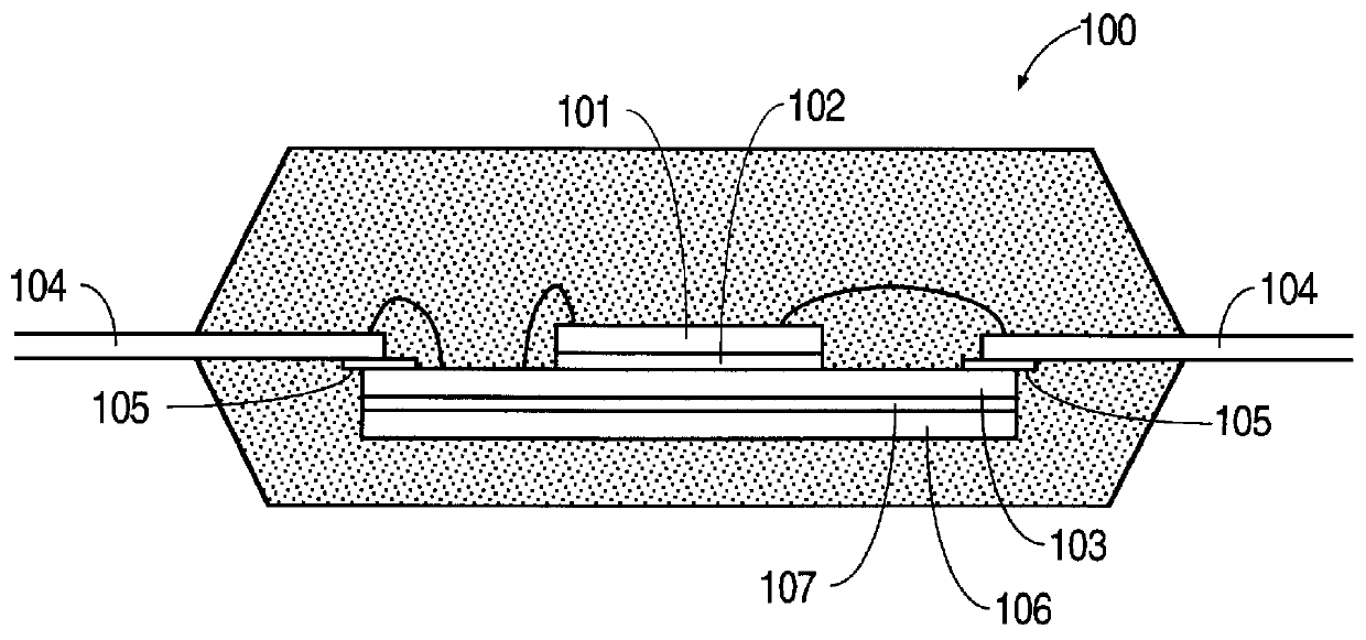
Leadframe with power and ground planes
a ground plane and leadframe technology, applied in the direction of semiconductor devices, semiconductor/solid-state device details, electrical apparatus, etc., can solve the problems of high speed operation, exacerbate the problem of switching noise and crosstalk, and give rise to noise (signal delays and signal distortions), so as to reduce the effect of effective inductance and crosstalk, and minimize the inductance and noise in power and ground paths
- Summary
- Abstract
- Description
- Claims
- Application Information
AI Technical Summary
Benefits of technology
Problems solved by technology
Method used
Image

Examples
Embodiment Construction
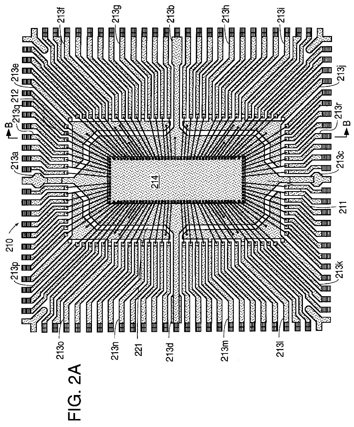
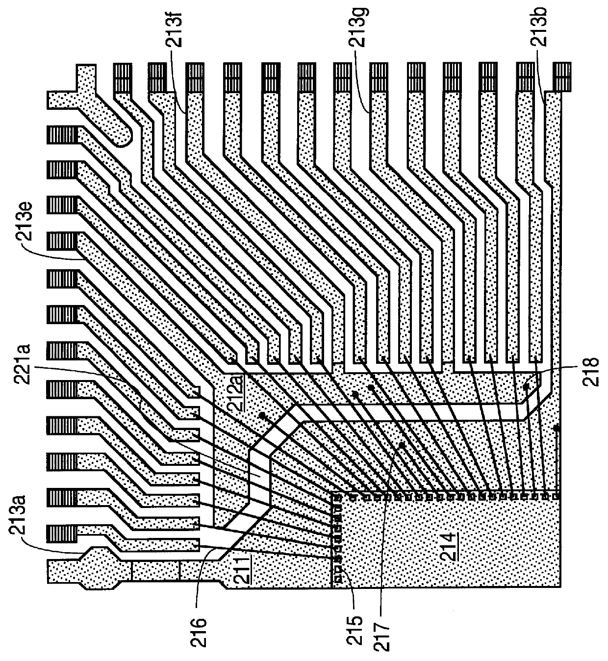
In accordance with the invention, a leadframe is provided for use with an integrated circuit package. FIGS. 2A and 2B are a plan view and detailed plan view, respectively, of a semiconductor die 214 mounted on a leadframe 210 according to an embodiment of the invention.
The leadframe 210 comprises a die attach pad 211, a ring 212 and a plurality of leads 213. (In FIGS. 2A and 2B, several particular leads are identified, e.g., lead 213a. All leads or a typical lead that may or may not be specifically identified will be referred to as leads or lead 213, though 213 does not appear as a numerical designation in the drawings.) The die attach pad 211 is formed approximately in the center of the leadframe 210. The ring 212 is formed generally around the periphery of the die attach pad 211 with a gap 221 separating the die attach pad 211 and ring 212. The gap 221 is necessary to ensure electrical isolation between the die attach pad 211 and ring 212. The leads 213 are formed generally around...
PUM
 Abstract
Description
Claims
Application Information