System and method for integrating a digital core with a switch mode power supply

a digital core and power supply technology, applied in the field of semiconductor circuits, can solve the problems of less than optimal linear voltage regulation cores or devices to provide these plural voltage domains from a single supply voltage, and the overall solution cost and power consumption may actually rise, so as to achieve the lowest possible cost, minimal heat dissipation and cost, and optimal power savings

Inactive Publication Date: 2005-09-06
CUFER ASSET LTD LLC
View PDF4 Cites 122 Cited by
  • Summary
  • Abstract
  • Description
  • Claims
  • Application Information

AI Technical Summary

Benefits of technology

[0006]The present invention is directed to a system and method for integrating a semiconductor die of plural power supply voltage domains with a switch mode DC-to-DC converter in an integrated circuit package. The invention discloses a system and a method to design and fabricate such an integrated circuit system in a single package to obtain optimal power savings, and minimal heat dissipation and cost. According to one embodiment, a semiconductor die is situated within the periphery of a lead frame adjacent to the switch mode power supply substrate. The substrate can comprise, for example, a ceramic material, or most economically, a fiberglass resin epoxy based laminate material such as FR4. In one embodiment, the semiconductor die is situated on the substrate adjacent to the integrated switch mode DC-to-DC converter. In one embodiment, a semiconductor die may receive power for its lower voltage supply pads through any DC-to-DC converter of the switch mode step-down variety in a closed-loop general solution implementation.
[0007]In the preferred embodiment, the present invention provides a superior means for optimally converting voltages to the correct domains for semiconductor die operation through synchronous step-down conversion. Furthermore, the present invention's substantial departure from prior art and significant novelty exists in the preferred embodiment wherein said switch mode synchronous DC-to-DC step-down converter is implemented in an open-loop configuration retaining precision based on semiconductor die power consumption characterization data, thus achieving the lowest possible cost for total solution of the system-on-chip.

Problems solved by technology

While this advancement brings the advantage of reduced core power consumption as a product of one-half the total gate capacitances times the gate voltages squared times the switching frequency, there arises the problem of regulation of these additional voltages.
Often both the system-on-chip designer and the top-level integrator, not having the time, resources, or background of experience in power supply design tend to choose simple-to-implement, but less than optimal linear voltage regulation cores or devices to provide these plural voltage domains from a single supply voltage.
The overall solution cost and power consumption may actually rise if this heat dissipated in the linear voltage regulator is great enough to require additional components to provide forced air convection cooling.
Also, the system-on-chip itself could require additional heat-sinking components or else suffer reduced reliability due to the implementation of a linear voltage regulator on-chip, thereby driving-up hidden costs of the total solution.

Method used


Image

  • System and method for integrating a digital core with a switch mode power supply
  • System and method for integrating a digital core with a switch mode power supply
  • System and method for integrating a digital core with a switch mode power supply

Examples


Embodiment Construction

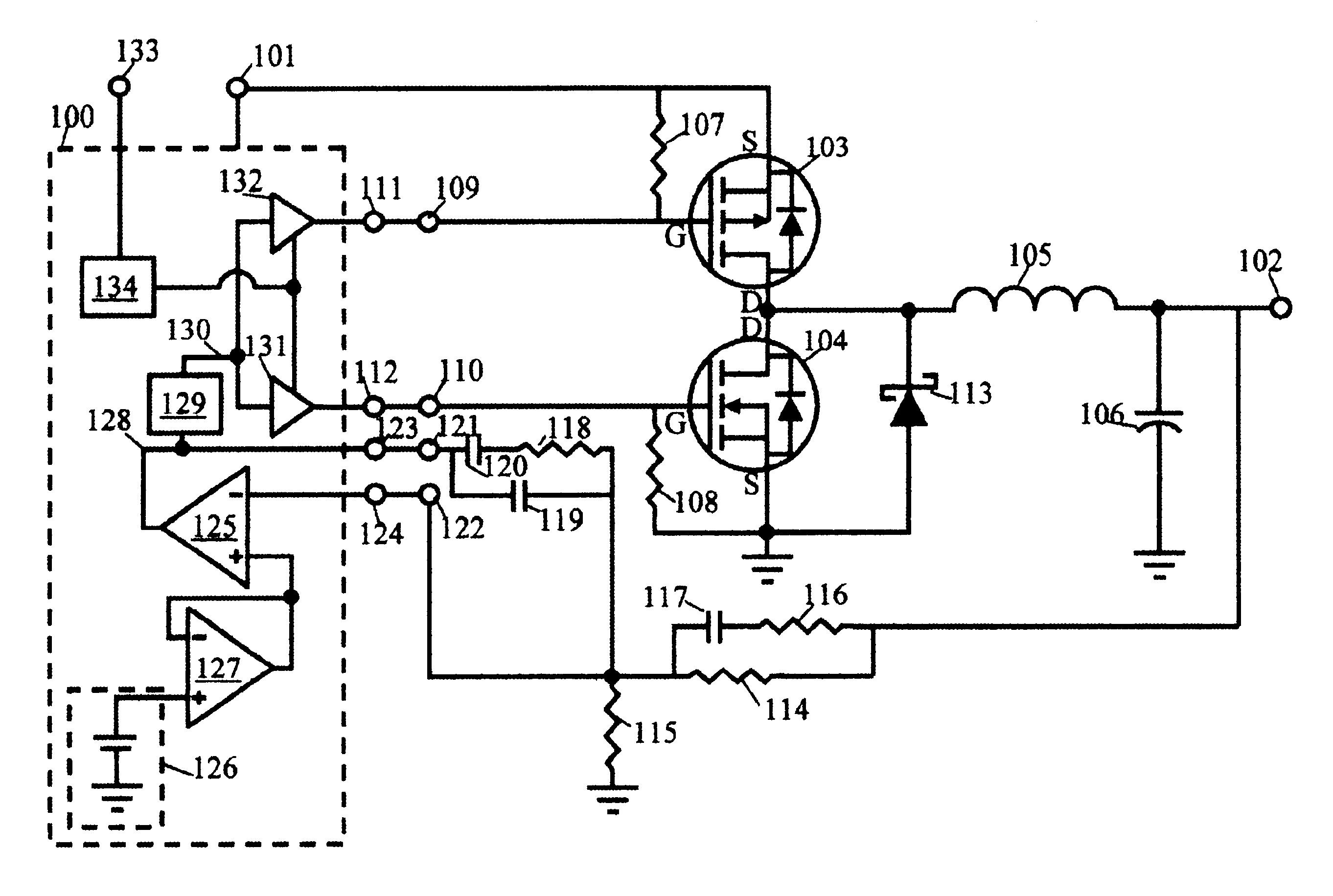
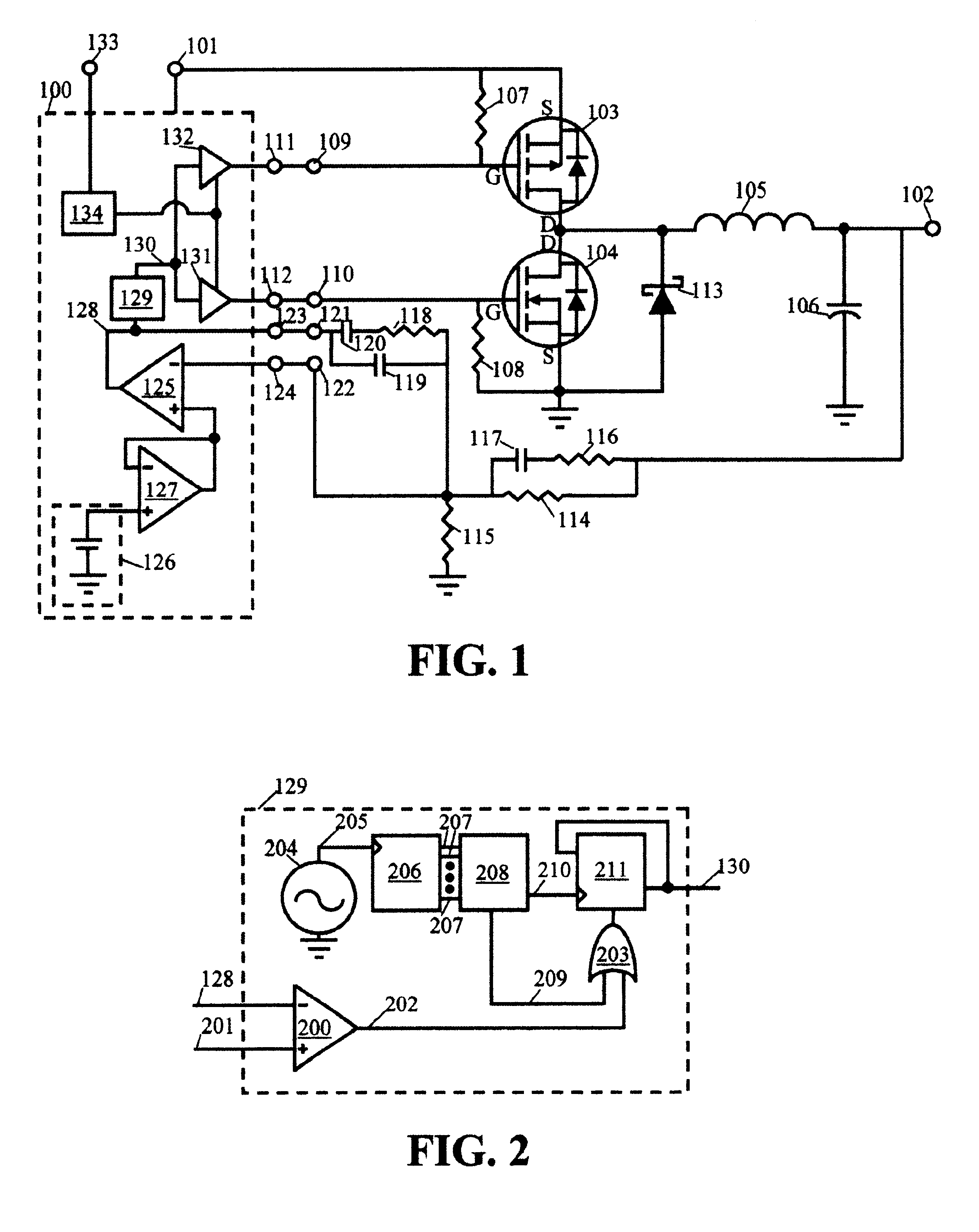
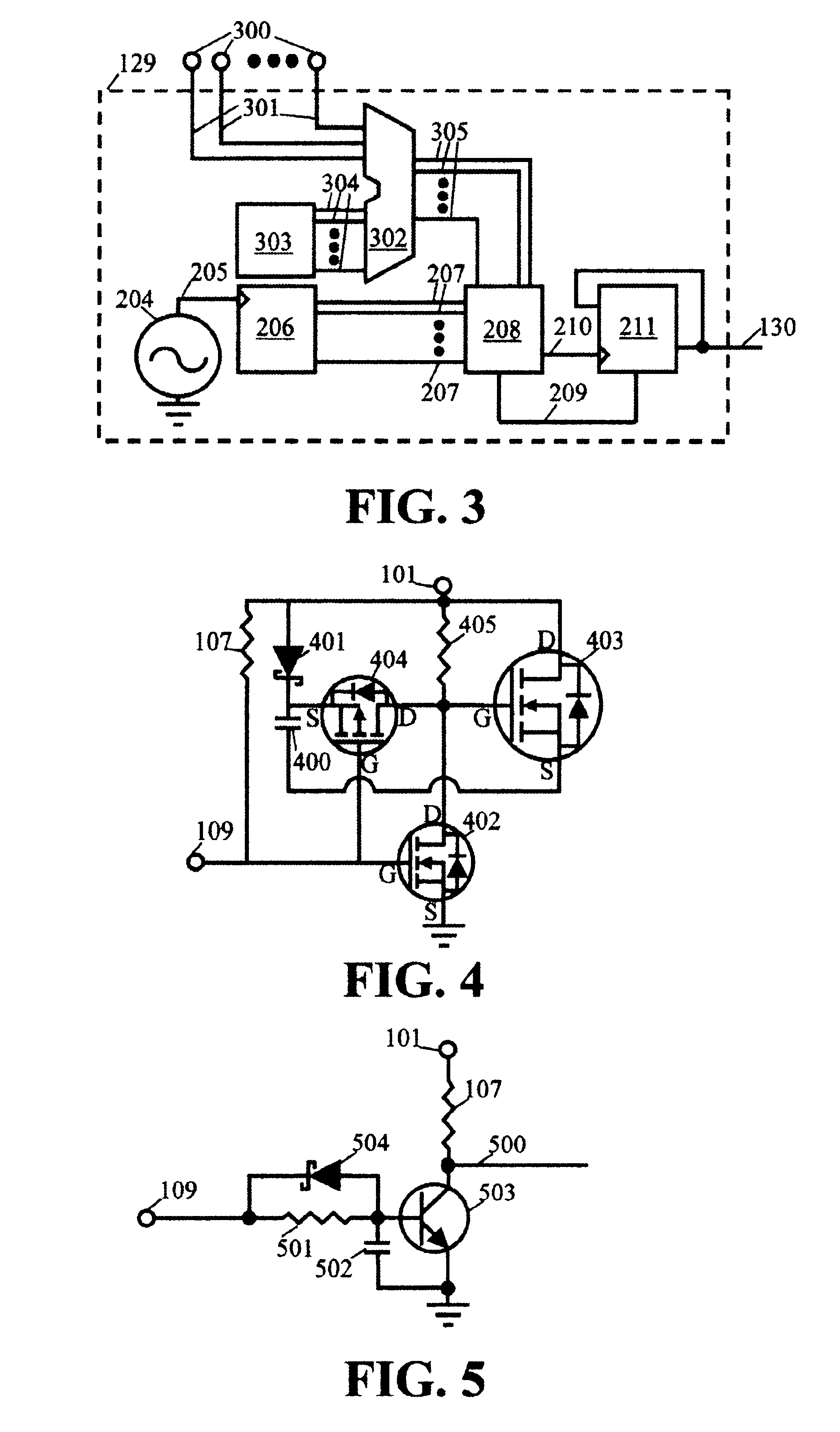
[0016]The present invention is directed to a system and method for integrating a semiconductor die of plural power supply voltage domains with a switch mode DC-to-DC converter in an integrated circuit package. The following description contains specific information pertaining to various embodiments and implementations of the invention. One skilled in the art will recognize that the present invention may be practiced in a manner different from that specifically depicted in the present specification. Furthermore, some of the specific details of the invention are not described in order not to obscure the invention. The specific details not described in the present specification are within the knowledge of a person of ordinary skills in the art. Obviously, some features of the present invention may be omitted or only partially implemented and remain well within the scope and spirit of the present invention.

[0017]The following drawings and their accompanying detailed description are dire...


PUM


Abstract

A digital core embodied within a semiconductor die that requires plural separate power supply voltage domains is situated within any of a variety of integrated circuit packaging technologies. Within the integrated circuit package including this semiconductor die also exists a switch mode DC-to-DC voltage converter, preferably a synchronous step-down regulator powering the entire integrated circuit from one supply voltage. The components contained within the integrated circuit package along with the semiconductor die include the switch mode power supply's power switching transistors, inductor core and windings, digital open-loop output voltage fixing circuitry, output capacitors and substrate for mounting said components when integrated within a packaging technology that does not already include a substrate.

Description

BACKGROUND OF INVENTION[0001]1. Field of the Invention[0002]The present invention is generally in the field of semiconductor circuits. More specifically, the present invention is in the field of semiconductor die packaging with integrated power supply voltage regulation.[0003]2. Background Art[0004]Advances in semiconductor integrated circuit fabrication processes and digital standard cell and semi-custom application specific integrated circuit, “ASIC”, design methodologies have given rise to digital and mixed analog and digital signal integrated circuits requiring separate power supplies for various parts including a unique voltage for the digital core power supply, and a second, unique power supply voltage for the input / output pad ring, and possibly a third power supply voltage for miscellaneous analog functions. While this advancement brings the advantage of reduced core power consumption as a product of one-half the total gate capacitances times the gate voltages squared times t...

Claims


Application Information

Patent Timeline
Patent Type & Authority Patents(United States)
IPC IPC(8): H02M3/00H01L25/16H02M3/158H02M3/04H02M3/157
CPCH05K1/0292H02M3/00H01L25/16H01L2924/30107H05K1/167H05K2203/171H01L2224/48091H01L2224/48195H01L2924/01015H05K1/0262H01L2224/45147H01L2224/49175H01L2924/12032H01L2924/3011H01L2924/00014H01L2924/00H01L2224/05553H01L2224/48137H02M3/003
Inventor GIZARA, ANDREW ROMAN
Owner CUFER ASSET LTD LLC
Why Eureka
Try Eureka