[0005]The present invention contrives to improve the focusing speed and portability of an automatic focus imaging system by reducing volume,
mass and / or
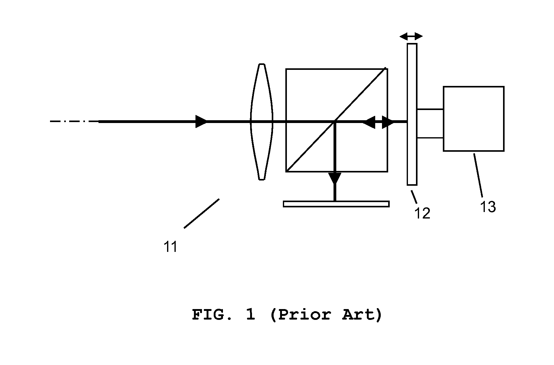
power consumption of the system. FIG. 1 shows a conventional automatic focus imaging system using the translation of a reflective surface. An
actuator is connected to the reflective surface such that the reflective surface moves to adjust focus. Since the optical system with automatic focusing function requires additional optical components including a reflective surface and an actuator, the optical system has larger volume and
mass than an optical system without automatic focusing function. To apply automatic focus imaging system to portable devices such as cellular phone camera, it is very important to reduce the volume,
mass and power consumption of the automatic focus imaging system and increase the reliability and focusing speed of automatic focusing function.
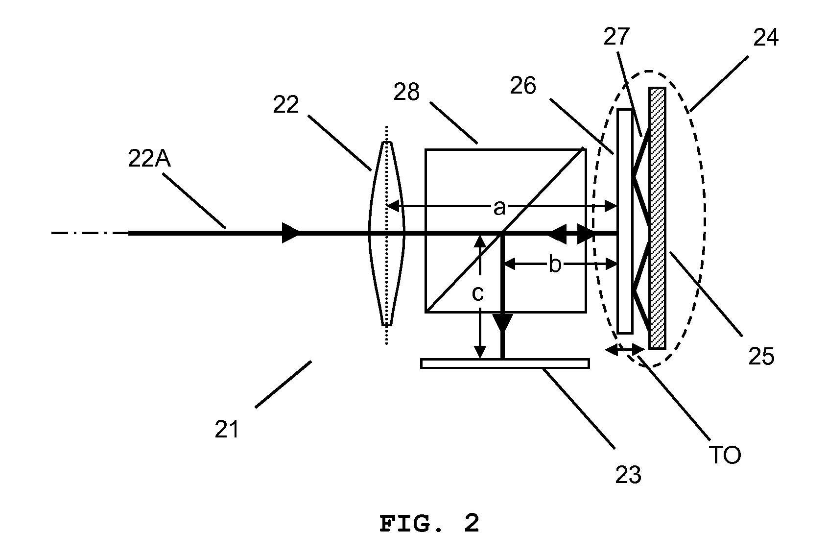
[0006]In the present invention, the automatic focusing function is performed by a Micro-Electro-
Mechanical System (MEMS) unit. The MEMS unit has a small volume and mass and low power consumption, and its operation is very reliable, precise, and fast. The MEMS unit for automatic focus includes at least one reflective surface and at least one actuation unit fabricated on the same substrate by
microfabrication technology. By fabricating the reflective surface and the actuation unit on the same substrate, the volume, mass and power consumption of the automatic focus imaging system of the present invention can be greatly reduced, which increases the portability and focusing speed of the automatic focus imaging system. In general, an actuator used for automatic focusing is required to provide several hundreds
micrometer of out-of-plane translation to a reflective surface. The out-of-plane translation is defined as a translation in the surface normal direction of the substrate while the in-plane translation is defined as a translation in the direction of an axis laying on the
substrate surface. The conventional MEMS devices are capable of providing out-of-plane translation to the reflective surface and have an
advantage of adding negligible volume and mass to the optical system. However, they have a limited range in the out-of-plane translation (typically only several micrometers) while having a
large range in the in-plane translation. In order to increase the range of the out-of-plane translation, the actuation unit of the present invention preferably comprises at least one micro-actuator and at least one micro-converter, wherein the micro-converter converts the in-plane translation of the micro-actuator to out-of-plane translation of the reflective surface. The micro-converter of the present invention allows large out-of-plane translation by converting the large in-plane translation of the micro-actuator into the large out-of-plane translation of the reflective surface. Preferably, the micro-actuator is actuated by electrostatic force. The micro-actuator can be a least one comb-drive using electrostatic force. The comb-drive can generate “coming and going” in-plane motion with a short
stroke. The combination of two comb-drives can be used as a micro-actuator, wherein two comb-drives generate in-plane revolution and the in-plane revolution is converted to large linear in-plane translation. Then, the large linear in-plane translation can be converted to the large out-of-plane translation by the micro-converter. The micro-converter comprises at least one primary end, which can be connected to the micro-actuator or the substrate. All structures in the MEMS unit including the reflective surface, micro-actuator, and the micro-converter can be fabricated on the same substrate by
microfabrication technology and the micro-actuator can be controlled by applied
voltage.
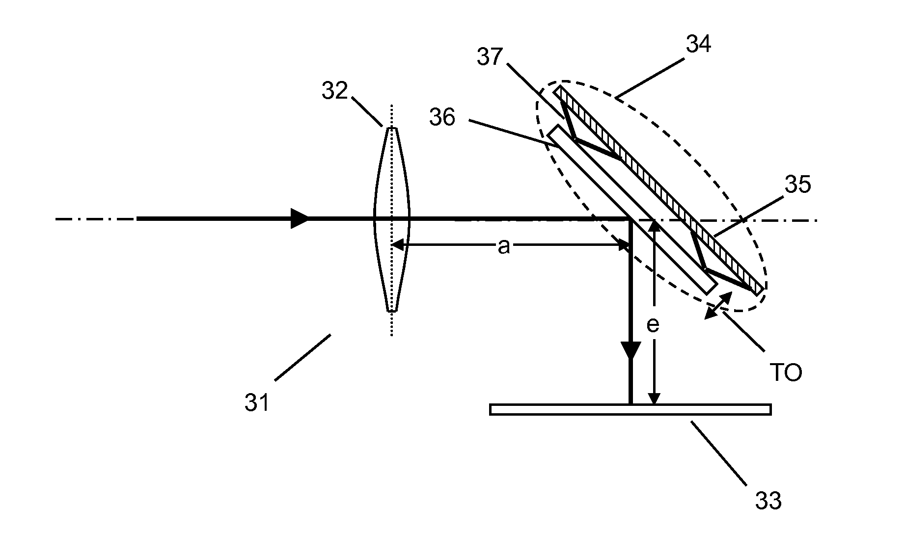
[0024]The portable optical devices have a high demand to provide high quality images while maintaining compactness. When the automatic focus imaging system uses a single reflective surface having a large area size,
distortion and twisting problems of the reflective surface can occur, which causes aberration. The present invention provides more robust and reliable automatic focus imaging system using a plurality of
reflective surfaces. The automatic focus imaging system comprises a lens unit, an image sensor and MEMS unit fabricated by microfabrication technology to improve the portability and focusing speed of the automatic focus imaging system. The MEMS unit comprises a substrate having a control circuitry, a plurality of
reflective surfaces movably connected to the substrate, and at least one actuation unit. The actuation unit comprises a micro-actuator disposed on the substrate and driven by the control circuitry to have in-plane translation and at least one micro-converter having a primary end. The primary end of at least one of the at least one micro-converter is rotatably connected to the micro-actuator and the micro-actuator with the in-plane translation exerts a force on the primary end of the at least one of the at least one micro-converter, wherein the at least one micro-converter delivers the force to the plurality of
reflective surfaces so that each of the plurality of reflective surfaces has a motion comprising out-of-translation motion. The MEMS unit is configured to change a distance between lens unit and the image sensor by controlling the out-plane translation of each of the plurality of reflective surfaces in order to form in-focus mage on the image sensor. The automatic focus imaging system of the present invention can have more robust and reliable automatic focusing function by using a plurality of reflective surfaces.

