
Pixel unit of ffs type tft-lcd array substrate

Active Publication Date: 2011-03-31
BEIJING BOE OPTOELECTRONCIS TECH CO LTD +1
View PDF2 Cites 10 Cited by
  • Summary
  • Abstract
  • Description
  • Claims
  • Application Information

AI Technical Summary

Problems solved by technology

In the conventional liquid crystal display, the image quality various notably when viewed from different view angles, which leads to the users' dissatisfaction with the product performance.

Method used


Image

  • Pixel unit of ffs type tft-lcd array substrate
  • Pixel unit of ffs type tft-lcd array substrate
  • Pixel unit of ffs type tft-lcd array substrate

Examples


Embodiment Construction

[0013]Hereinafter, the embodiments of the invention will be further described with reference to the accompanying drawings.

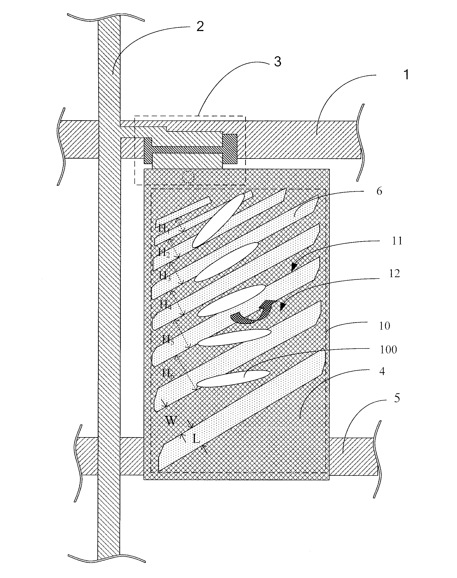
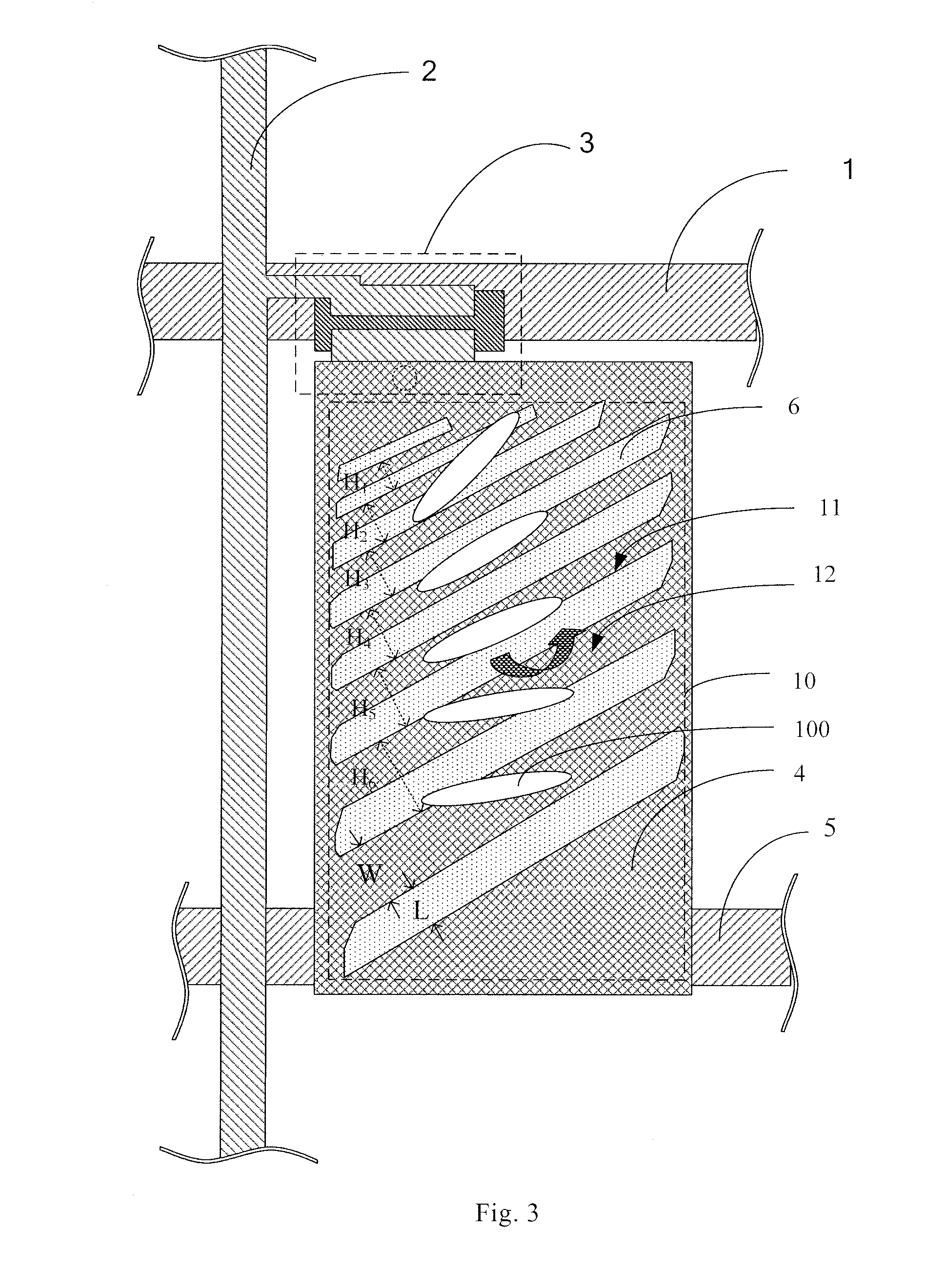
[0014]FIG. 3 is a schematic plan view for a pixel unit of an FFS type TFT-LCD array substrate according to an embodiment. As shown in FIG. 3, the FFS type TFT-LCD array substrate comprises a plurality of pixel units. Each pixel unit comprises a transparent substrate, a gate line 1, a data line 2, a thin film transistor (TFT) 3, a pixel electrode 4, a common electrode line 5 and a common electrode 6. The gate line 1 and the common electrode line 5 are provided on the transparent substrate transversely, and the data line 2 is provided on the transparent substrate longitudinally. The TFT 3 is provided at the intersection between the gate line 1 and the data line 2. The TFT 3 is an active switch element for controlling the pixel electrode 4.

[0015]In FIG. 3, the pixel electrode 4 is a slit electrode, and the common electrode 6 is a plate electrode. The common electrod...


PUM


Abstract

A pixel unit of an FFS type TFT-LCD array substrate comprises a slit electrode. The slit electrode comprises at least one slit unit, a direction from one side of the slit unit to the opposite side of the slit unit is defined as a first direction, the slit unit comprises a plurality of slits, extending in a same direction and arranged along the first direction, and electrode parts between two adjacent slits. The sum of the width of each electrode part and the width of a slit adjacent to the electrode part at a side in the first direction increases gradually along the first direction.

Description

BACKGROUND OF THE INVENTION[0001]Embodiments of the invention relate to a pixel unit of a fringe field switch (FFS) type thin film transistor liquid crystal display (TFT-LCD) array substrate.[0002]TFT-LCDs have been an important type of flat panel displays (FPDs). TFT-LCDs can be classified into a vertical electrical field type and a horizontal electrical field type depending on the direction of the electrical field by which liquid crystal is driven. For a vertical electrical field type TFT-LCD, a pixel electrode is formed on an array substrate while a common electrode is formed on a color filter substrate. For a horizontal electrical field type TFT-LCD, both a pixel electrode and a common electrode are formed on an array substrate. Therefore, an additional patterning process for forming the common electrode is required when a horizontal electrical filed type TFT-LCD array substrate is manufactured. A vertical electrical field type TFT-LCD comprises a twist nematic (TN) type TFT-LCD...

Claims


Application Information

Patent Timeline
IPC IPC(8): G02F1/1343
CPCG02F2001/134372G02F1/1343G02F1/134372
Inventor PARK, HANJUN
Owner BEIJING BOE OPTOELECTRONCIS TECH CO LTD
Learn More